At Intel Vision 2024, we saw the Intel Gaudi 3 AI accelerator. This is Intel’s newest dedicated AI accelerator in a very hot market. The new Gaudi 3 is a big leap over the previous generation Gaudi 2, which we have seen before, and is set to go into volume production later in 2024.
As a quick note: I attended the Intel Vision 2024 as an “Influencer.” The press was not invited, but analysts were. The event is being held about 25 min from the STH studio in Scottsdale, so that is how I got a badge. If you want the sub-30 second short on our new shorts channel, here you go:
Intel Gaudi 3 128GB HBM2e AI Chip in the Wild
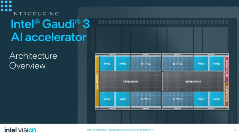
Of course, most folks like to see specs, and the Gaudi 3 is an interesting part. The new part still uses HBM2e but is using eight stacks to achieve 128GB of capacity. Intel has up to 1.835PFLOPS of FP8 compute. It should also be noted that simply supporting FP8 is non-trivial as some accelerators do not support it at this point. The new part has 64 tensor processor cores and 8 matrix math engines.
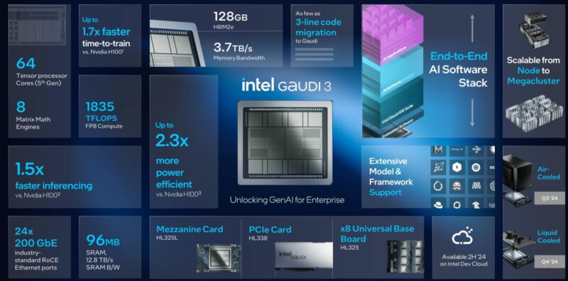
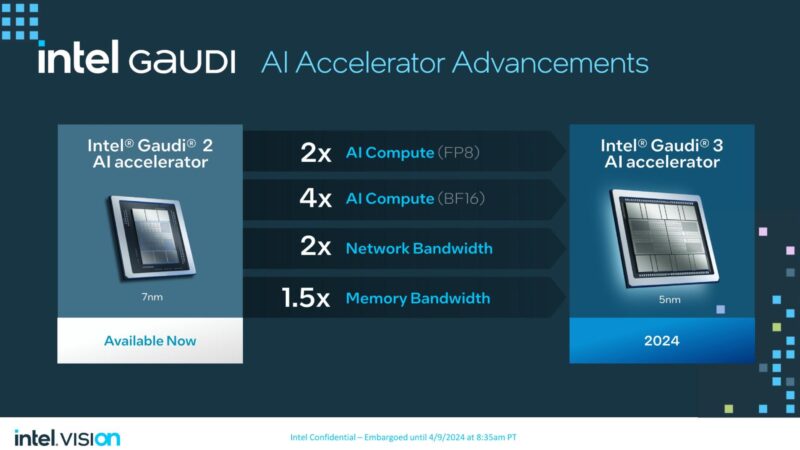
We have been tracking Habana’s Gaudi since 2019, and the company later in 2019 was acquired by Intel when it had its Gaudi 1 generation. That was at the point that Nervana was still around and a lot of the action was happening around Facebook’s choice for AI acceleration. Since 2019’s Intel acquisition, there was a Gaudi 2 generation that Intel started putting effort behind in late 2022 as AI took off. The Gaudi 3 is the successor with huge upgrades in compute and bandwidth, and a shrink from 7nm to 5nm.
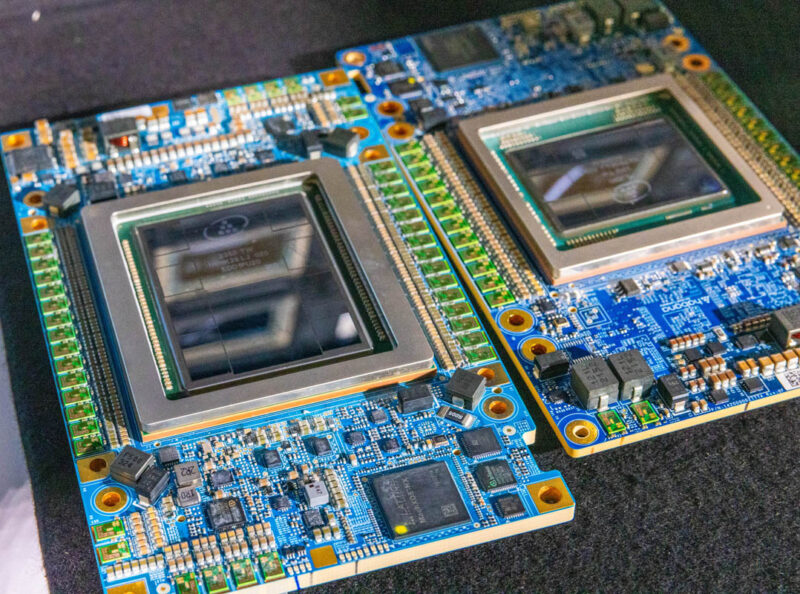
Just for some sense of scale as to how much bigger Gaudi 3 is, here is Gaudi 3 next to Gaudi 2.
Here is Gaudi 2 and Gaudi 3 in hand. It is plain to see when you are standing next to them that the Gaudi 3 silicon package is much larger.
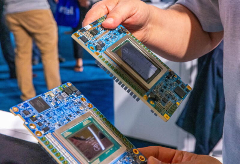
On that silicon package, there are two dies, each with 48MB of SRAM, 16 tensor processing cores, and a media engine. Something that Habana Gaudi 1 did, and we have seen continue, is that Gaudi 3 uses Ethernet to scale up and out. In this generation, that means the 24 network interfaces are 200GbE up from 100GbE in Gaudi 2 and only 10x 100GbE in Gaudi 1. Intel uses Ethernet as the interconnect between AI accelerators in a chassis, but also to scale out to multiple AI accelerators in a data center. Compare that to NVIDIA with NVLink/ NVSwitch, Infiniband, and Ethernet in a HGX H100 platform.
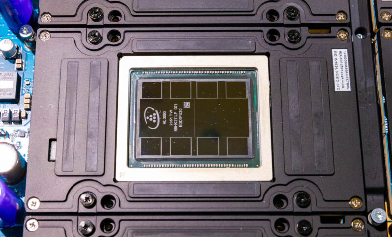
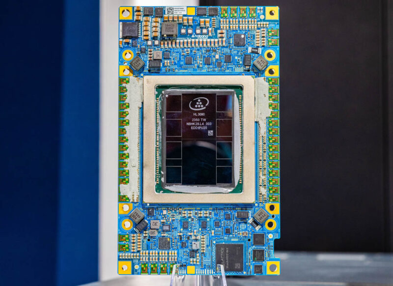
Here is a closer look at the die. The thermal paste is there because this was a working card that was pulled. If you are wondering what is between the 8x 16GB HBM2e packages, we were told that is filler silicon to make the structure of the package.
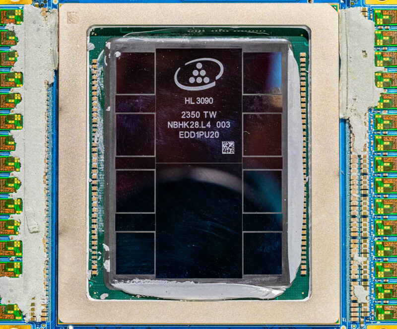
One can also see the line between the two pieces of silicon that make up the main compute, SRAM, and networking portion of the AI accelerator.
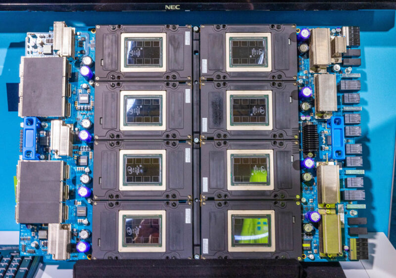
Of course, a single AI accelerator today with LLM’s is less exciting. What is more exciting is a collection of AI accelerators. Here is an OCP UBB with the 8x Intel Gaudi 3 OAM accelerators. All are listed at 900W each, but we heard there may be more room with liquid-cooled variants. TSMC has gotten decent voltage frequency scaling and NVIDIA has been taking advantage of that as well. The system below is around 7.2kW+ of accelerators, not taking into account other components.
Here is the OAM package bottom for the Gaudi 3.
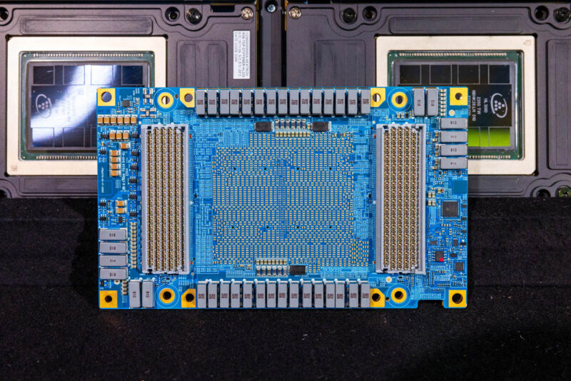
Gaudi 3 using Ethernet to scale was a key concept of Habana. The idea was that network admins fundamentally do not want to manage many types of data fabrics. Ethernet is ubiquitous so the aim was to use that, and this was before the idea of UltraEthernet came about. Of course, in 2024, network switch speeds are so much faster today with a modern 51.2T switch that can handle a ton of 200GbE devices. In 2019, with Gaudi 1, when 32-port 100GbE was still decently high-end, the network bandwidth and topologies were a bit more limited. The OAM package above takes 21 of the 24 lanes and uses 3x 200GbE to connect to each of the other seven OAM packages. The remaining 3x 200GbE links are then fed to OSFP connectors at the rear of the chassis.
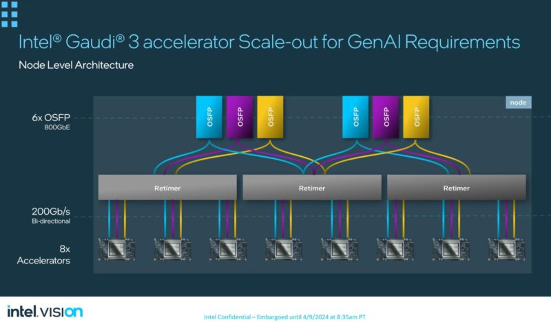
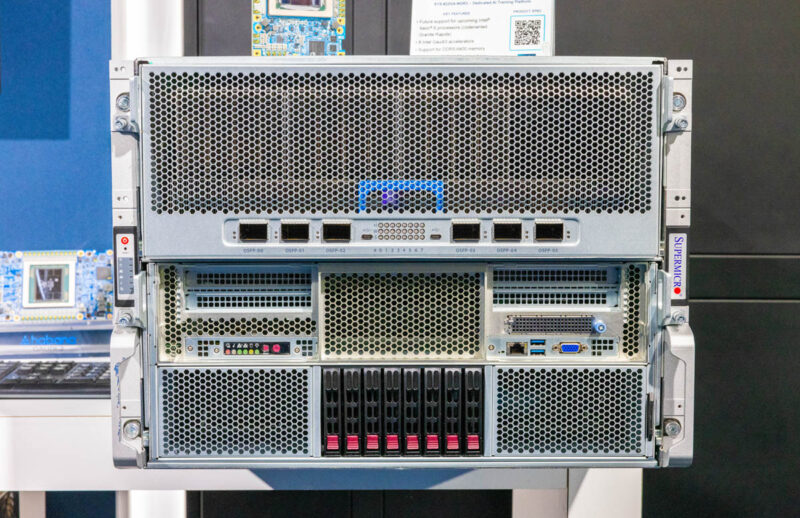
We saw a Supermicro X14 Gaudi 3 platform at Intel Vision 2024. That platform has six OSFP connections on the top where the Gaudi 3 OAM UBB resides. That should help map to the diagram above.
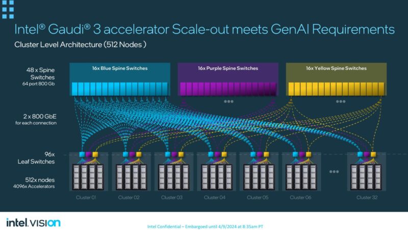
Those six OSFP ports can then be connected to switches and scale-out topologies built. Intel color-coded the networks in its materials to help better illustrate this. The benefit here is that building big Ethernet networks is fairly well understood.
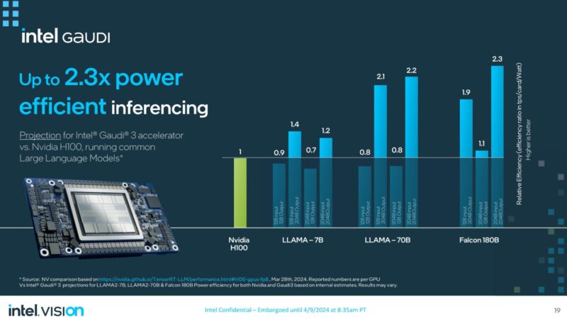
Intel says that the new Gaudi 3 is more power efficient, and sometimes faster than a NVIDIA H100 in inferencing. Our sense is that Gaudi 3 is going to find its home in the AI inference market.
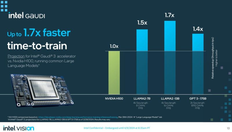
At the same time, Intel Gaudi 3 can also offer faster training than the NVIDIA H100. While the NVIDIA H200 is announced, we are still a bit from seeing training numbers for that as it starts ramping in volume production, and then later this year the NVIDIA Blackwell products will see another jump. Gaudi 3 is really competing on price here. The power efficiency message will be more powerful later in 2024 when organizations have to look at the power footprints they have and decide when to keep or retire machines to free up power capacity.
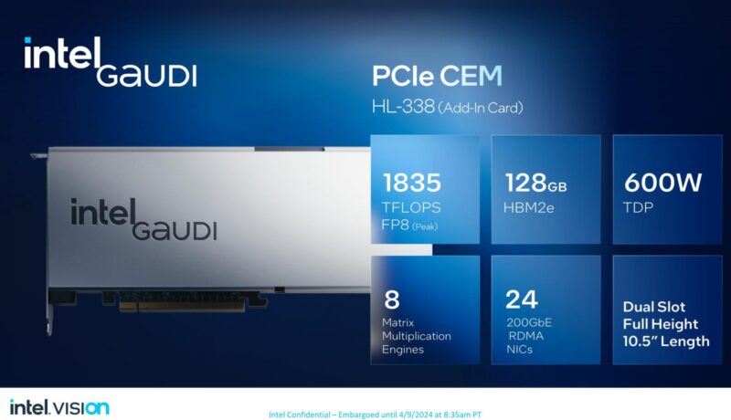
To that end, Intel also has the Gaudi PCIe CEM, the HL-338. This is an add-in card with a 600W TDP. It takes a lot from chassis to go from the 300-350W PCIe accelerators of just a year or two ago to 600W TDP today.
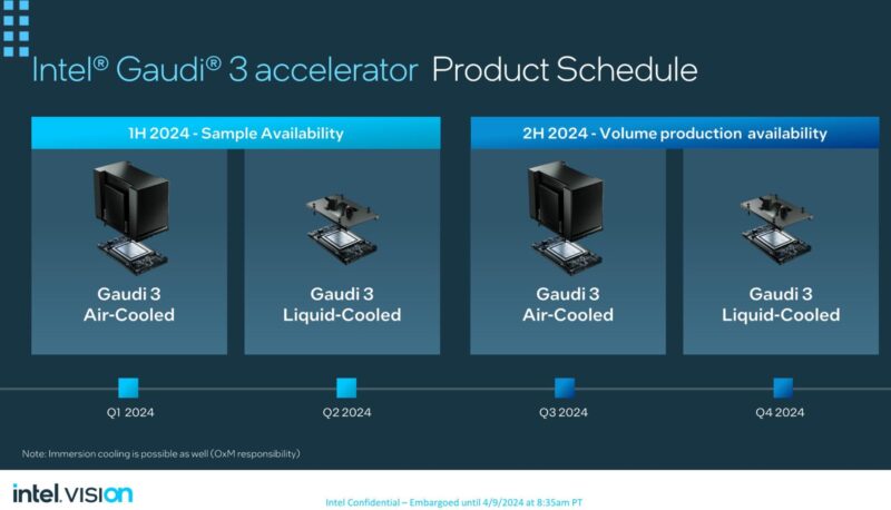
All of these accelerators are sampling in the first half of this year. The air-cooled and liquid-cooled variants will go into production in the second half of this year. That ties to the Granite Rapids-AP Xeon 6 Supermicro platform shown above.
The important thing to remember is that these will be contemporaries of the NVIDIA H200 and Blackwell, so Intel will likely offer them at substantially lower cost than NVIDIA. Next up, in 2025 is Falcon Shores, which will be a GPU architecture designed for AI as well. Intel says that it will be making the transition easy for users of Gaudi 3.
Final Words
Overall, the Intel Gaudi 3 is a big step up with more memory, more compute, and faster interconnect.
The market needs more compute, so the Intel Gaudi 3 will sell well. If you saw our Touring the Intel AI Playground Inside the Intel Developer Cloud piece, since 2023 Intel has been supply constrained on Gaudi 2. As a result, they are selling the parts and putting them in the Intel Developer Cloud to both try and run production workloads.
Hopefully, later in 2024, we get to check out systems with the new parts.


What are those small Green PCBs/chips on most od the edges when looking at the accelerator from above?
@M, the SER-DES for the PCIe x16 and the 200 GbE x24.
Yawn no CUDA equals no developers and no software. Nice brick.
The fact that there won’t be a Gaudi 4 but just Falcon Shore means no one will invest in making software for it.
That was honest from Intel to say there won’t be a follow up, but that also ensured no sales.
@Ziple
Awesome that non computer science people are writing here.
I encourage everyone to learn about CS. It’s fun to work in the industry.
Apart from that:
It is called an API.
An API is used to abstract from the actual hardware.
The very basics of computer science is being able to abstract from machine details such as instruction sets.
Intel’s counterpart to CUDA (which is also just an API also) is OneAPI / Khronos SYCL. Or PyTorch or … or…
Also there are semi-automatic conversions from CUDA to SYCL.
Imagine having to support every hardware on this planet by using assembly / machine instructions.
Yes, that would be bad. I agree
Apart from that I don’t know if there are customers for Gaudi 3 and whether it will be a success.
But I highly doubt you can judge that either because you don’t seem to have enough knowledge.