
At FMS 2026, we saw two neat demos on BiCS NAND. For those who do not know, BiCS NAND is a joint endeavor by Kioxia and SanDisk. Both companies showed BiCS NAND under a microscope at FMS 2026 and we took photos of them.
This is BiCS NAND Close Up from Kioxia and Sandisk
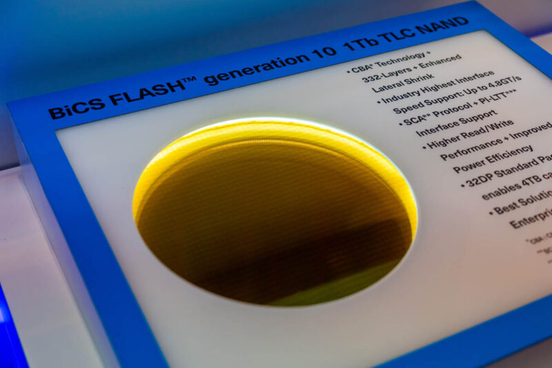
Starting off, here is the wafer that Kioxia showed of the BiCS FLASH Generation 10 1Tb TLC NAND. It uses CBA technology and has 332 layers.
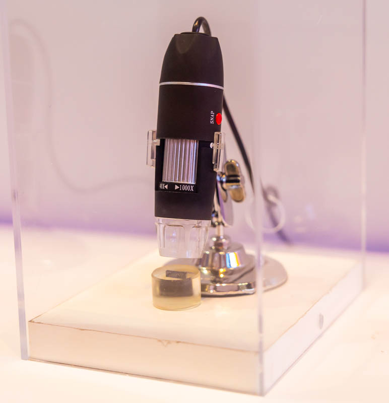
Next to it, you can see a die cross section and a microscope.
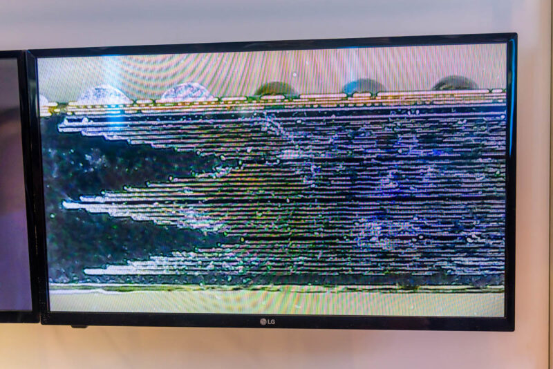
This is just a really neat cross-sectional view of how the NAND is built. You may think everything is straight up and down, but on the left side you can see that they are actually offset a bit. On the top, you can see the package balls as well for a sense of scale.
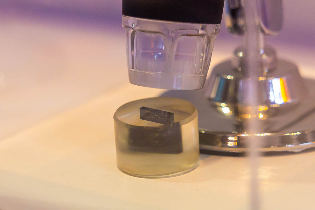
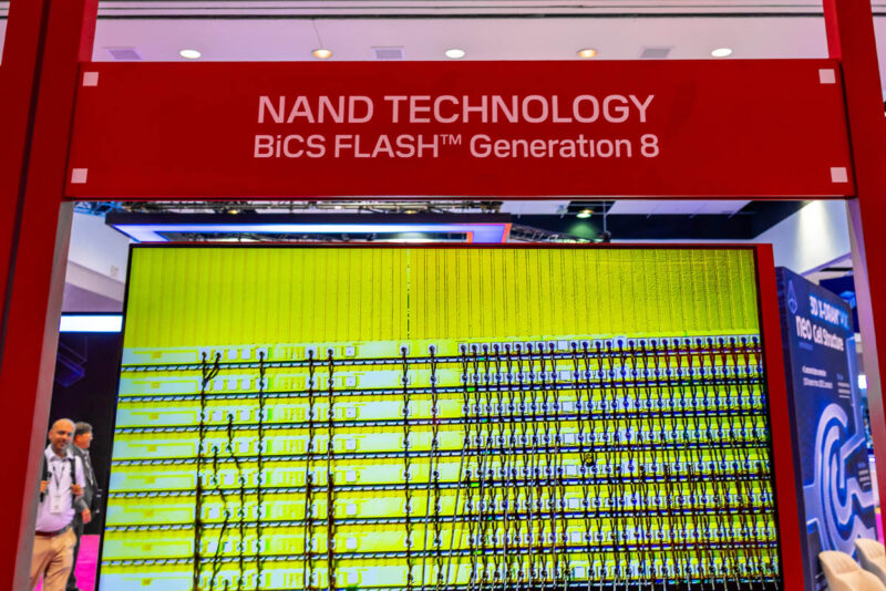
That brings us to Sandisk’s booth with BiCS FLASH Generation 8 on display under a microscope.
Sandisk also had a wafer on display.
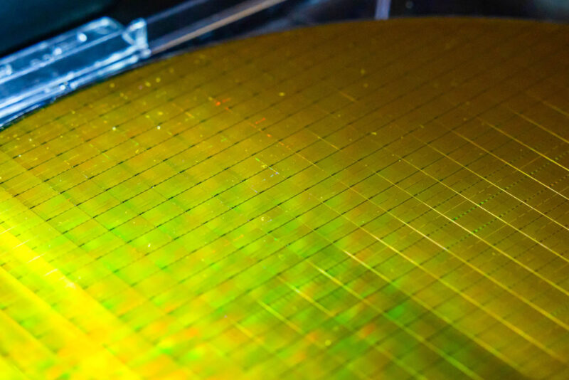
We captured this shot of the package that was under the microscope.
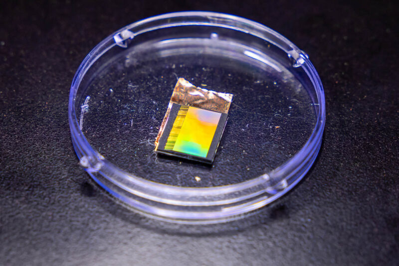
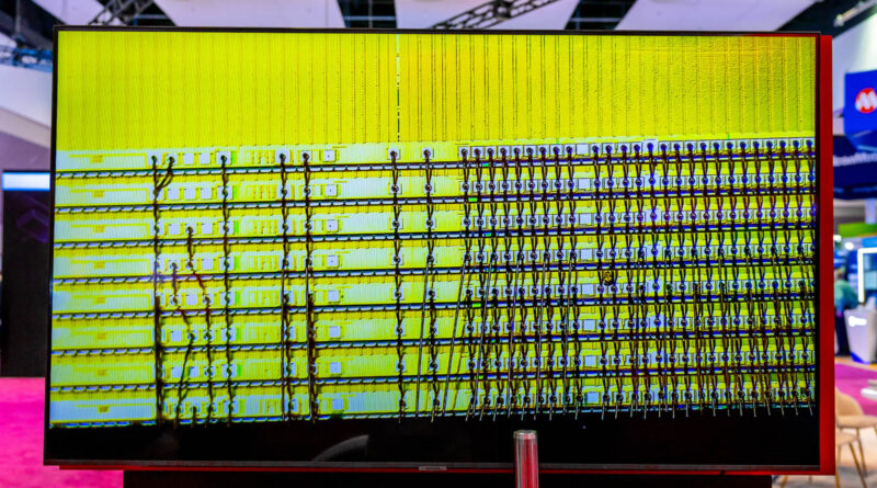
Here, you can see the tiny wires going between the different layers. You can get a sense of just how small those wires are between the layers, and they are something you would not normally see even just looking at the package from a distance.
Later, we went back and saw a different view of the package and the cells storing data. In this case, it was more like what could be storing data if the package was not opened to show under the microscope on the show floor.
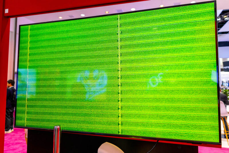
It is quite amazing to see these show floor demos where you can see the actual NAND packages opened up.
Final Words
NAND is a hot topic today as the demand is through the roof with AI. We often take for granted how challenging the engineering is to fit higher capacities and higher speeds within the NAND packages that go in our SSDs and devices. So much so that we have seen the microscopes out on NAND before at shows, but we had not covered it. Then we realized we had taken the photos, and many people have not seen these kinds of demos before. Hopefully, you enjoyed getting a look.