When it comes to high-end switches, we have been trying to show the gear more often on STH over the past few years. While we have focused on server CPUs for more than a decade, modern switch ASICs are pushing I/O well beyond a modern CPU. We recently had the opportunity to get a Broadcom Tomahawk 4 switch ASIC loose to show our readers. This is a super popular chip, but Broadcom has little marketing so folks have likely not seen it.
Broadcom Tomahawk 4 64-port 400GbE Switch Chip
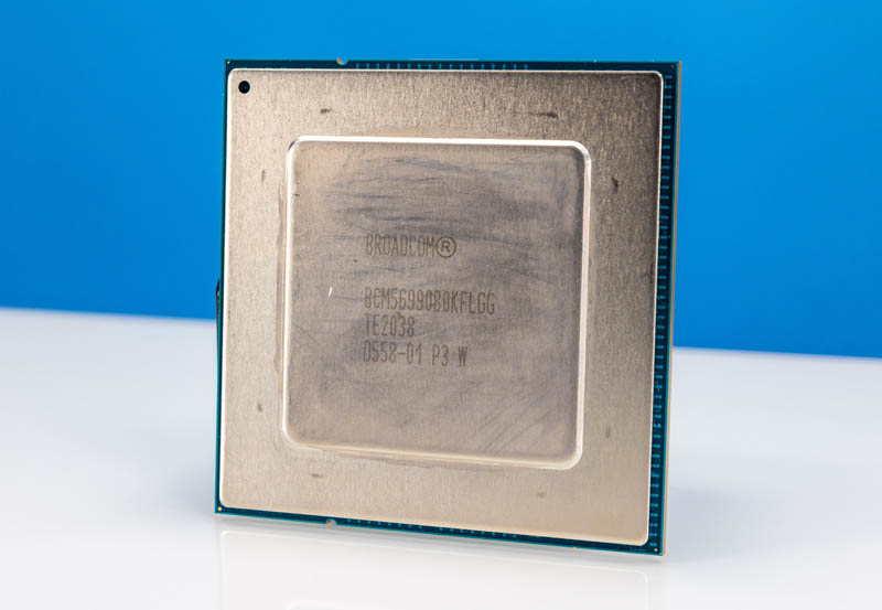
This giant chip is the Broadcom Tomahawk 4. It sports massive bandwidth and is extremely popular in the industry.
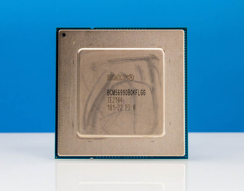
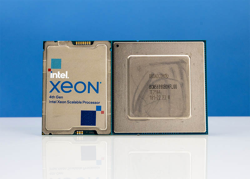
Showing the chip on its own does not necessarily convey just how large it is. Here is a 4th Gen Intel Xeon Scalable “Sapphire Rapids” server CPU next to the Broadcom Tomahawk 4.
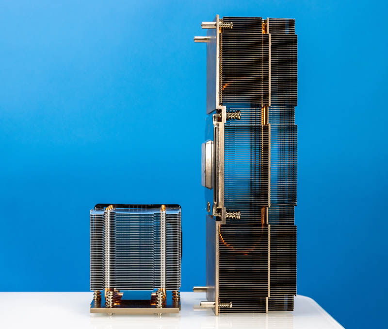
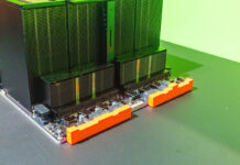
While you might be tempted to think that the Tomahawk 4 is a low power chip, here is a Dynatron J12 for AMD EPYC SP5 Genoa next to the heatsink from the FS 64-port 400GbE switch covering its Broadcom Tomahawk 4 chip.
Of course, the main feature of the Tomahawk 4 is to provide connectivity. 64 ports of 400GbE mean we have a lot of I/O pins. Here is the bottom pad side of the Tomahawk 4.
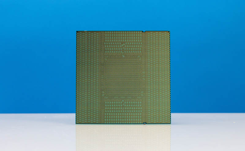
The Tomahawk 4 resides in a LGA8371 socket. This one appears to be made by TE Connectivity. That is a lot of pins!
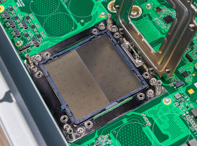
Since we did not have the right suction cup for this, instead, here is hand pulling the Tomahawk 4 from the LGA8371 socket. DO NOT DO THIS!
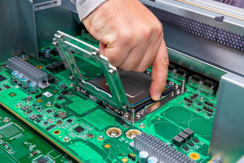
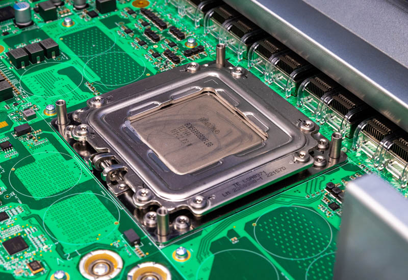
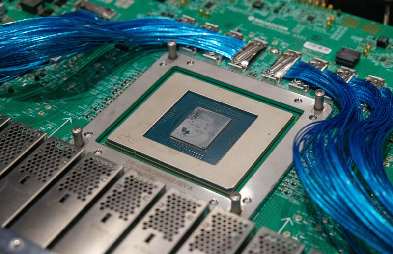
Here is the chip in the socket with the socket retention open. The retention here is more akin to an AMD EPYC 7001-7003 Naples/Rome/Milan rather than a Genoa or Xeon since the retention bracket is what is providing the force needed to keep the chip in. Modern server CPUs use the heatsink for the necessary clamping force.
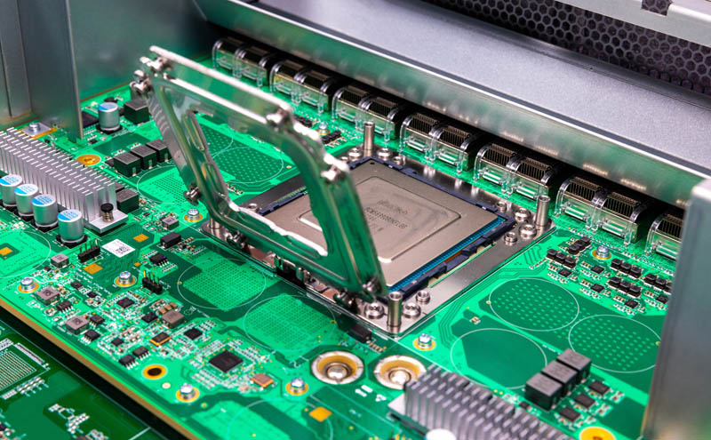
Here is the Tomahawk 4 in the socket.
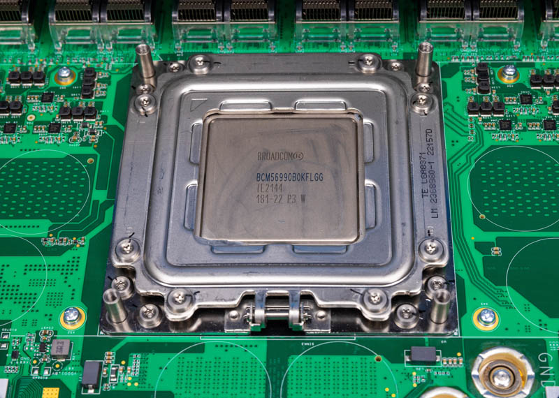
Here is another glamor shot just because folks rarely get to see this.
This is the opposite side.
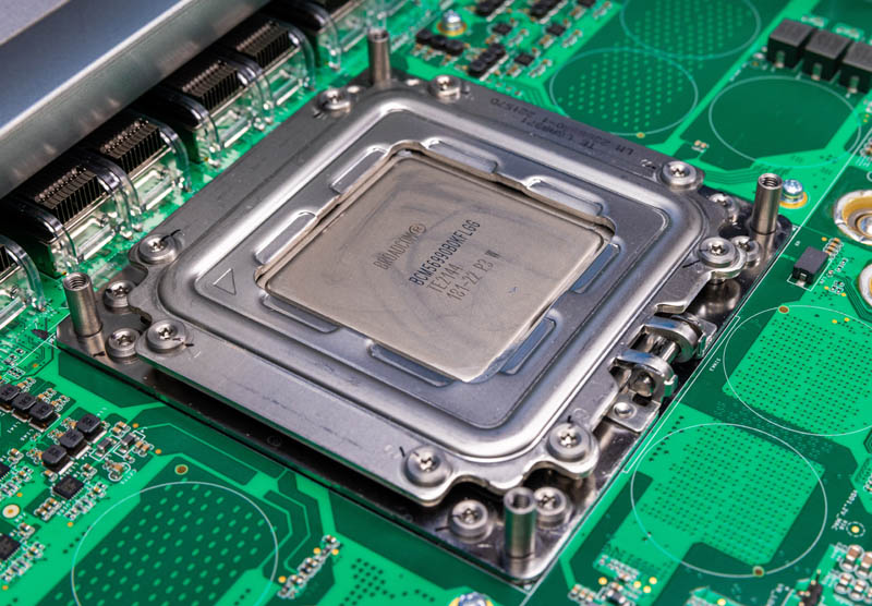
That is probably something one does not see everyday. Most switches we have reviewed have the switch ASICs soldered onto the main switch PCB. This was different which allowed us to show this view.
Final Words
One may have noticed that we also now have a loose Tomahawk 4 that has found its way onto the STH YouTube set’s background. This was so cool that once we saw it, we had to find a way to get one for the set.
Not having the proper equipment, but having done chips like the Ampere Altra/ Altra Max helped prepare us to do this installation. This is a big socket and we expect server CPUs to start using higher pin count sockets in 2023/ 2024.
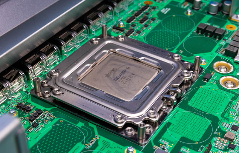
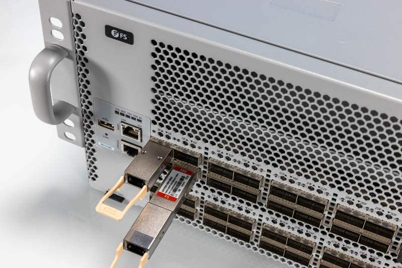
If you saw our recent NVIDIA ConnectX-7 400GbE and NDR Infiniband Adapter Review from PNY or the FS 400Gbase-SR8 400GbE QSFP-DD Optical Transceiver Review you will have seen the switch we found this in. We are going to have the review of the FS 400GbE switch once the video is done editing.
While 400GbE is interesting, Broadcom already has the 800GbE generation Tomahawk 5 that we saw at OCP Summit 2022, and with co-packaged optics.
Hopefully, you enjoyed this look at hardware very few folks in the industry ever get to see. We are going to continue working on getting you looks at new networking hardware over the rest of this year.


Wow! LGA-8371… Definitely a mainframe-sized processor and socket! That’s quite a few more pins than my POWER5+ MC-TCM and even Intel’s upcoming LGA-7529 Xeon socket! I would definitely be a happy camper if I got one of these monsters into my CPU collection! :-)
By the way, if anybody sees my comment and asks, what I mean by “mainframe-sized” is the processor, or rather its package and socket, is so physically large that you’d be forgiven if you expected to see and assume it came out of a large mainframe computer and not a network switch, server or single-user workstation. :-)
Literally lol’d at the heatsink
So big! Always thought these are soldered to the PCB.
Out of curiosity; what is the incentive behind socketing in this case? Does Broadcom have a CPU-like collection of pin and board compatible parts with significantly different prices and capabilities that makes being able to configure relatively late in production, not during surface mounting, valuable? Is BGA reworking something of that size just so intimidating that the socket is there to protect the (presumably rather more expensive than the mainboard) silicon if there’s a defect elsewhere in the system?
needs more heatsink
Wait…Broadcom is the company not soldering things down so they can be replaced etc….? Where am I? Who are you? What is this?
Oh lawd he coming
@fuzzyfuzzyfungus likely they did the socketing to mitigate mechanical stress during thermal expansion. It would be too hard to match the base-board with such long chip package – and the balls would very quickly tear off.
This is not a system, where the thermals are brought up slowly and evenly, there is a significant hotspot and a large cold plate. It would not work with soldering.
The largest soldered BGA’s we worked with are Stratix10 GX 10M fpga devices – 4938 pins in a 70×74 mm package. Not sure if that special dual-die BGA Xeon AP is larger or not.