Getting to Cut Open Mainframes Down to the Silicon
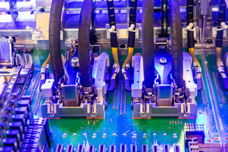
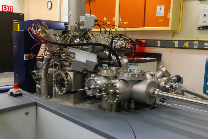
At the event, we were able to see the SMP cables connected with the liquid cooling blocks. IBM is actually doing something well beyond what we see from lower-end server and GPU providers. Still, with both the SMP cables on the top, and the complex liquid cooling blocks, there is a lot more going on, and these are systems expected to run at 99.999999% uptime or only have around 1 second of downtime per year. They are even tested to operate through 8.3 magnitude earthquakes.
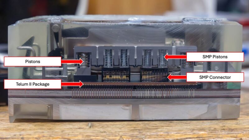
For some sense of what is going on here, this is a cutaway model of the package in its socket.
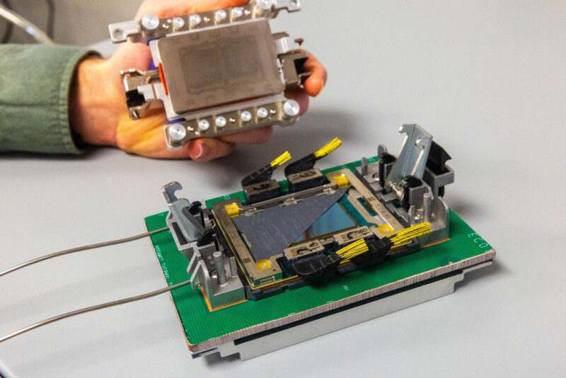
There are certainly big differences between this and a standard servers, or even GPU servers. Here you can see the spring loaded pistons that help to evenly distribute pressure across the socket.
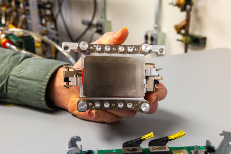
While up at IBM’s Fishkill lab, we were also able to see samples that were encased in blocks and then cut in a cross section for analysis. Here is one of the sockets above cut along the SMP connectors on the package, and you can see the socket and board below it as well.
I asked about the pistons. Apparently they are there to apply even pressure to not just the cooling solution to the CPU package, but also to keep the SMP cables in place.
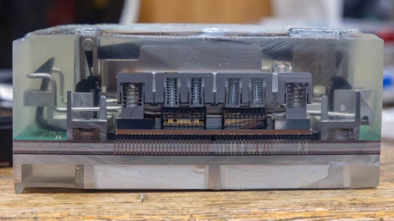
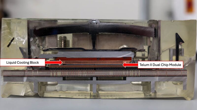
Another cross section was this one where we can see the actual Telum II chips and the liquid cooling block.
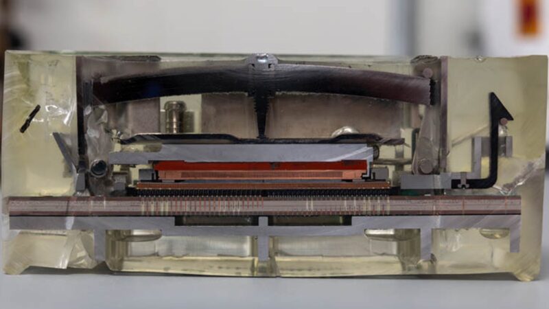
Here you can see the two Telum II chips then the copper liquid cooling block with the fluid channels going through it. There is also a void that is filled between the liquid cooling block and the rest of the assembly. In standard server liquid coolers, this would just be a metal block but IBM is going through the extra effort to ensure even pressure and reliability.
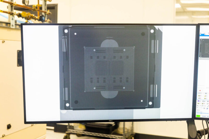
While cutting things open helps expose big parts of the socket, IBM has machines that can non-destructively look inside parts. For example, here is one of those SMP connectors from above but where one of the wires was not connected internally. You can see it on the bottom left image at the top of one of the middle wires.
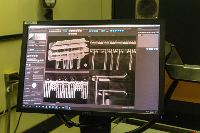
This view can also be rotated to see inside. A fun fact I learned. People actually buy old versions of these machines to look inside unopened trading card and baseball card packages looking for valuable cards without opening the packs.
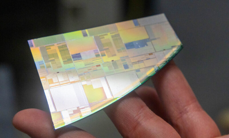
Of course, IBM had more traditional ways to look at the packages.
That also included a better look than we got at the z17 launch event of a wafer.
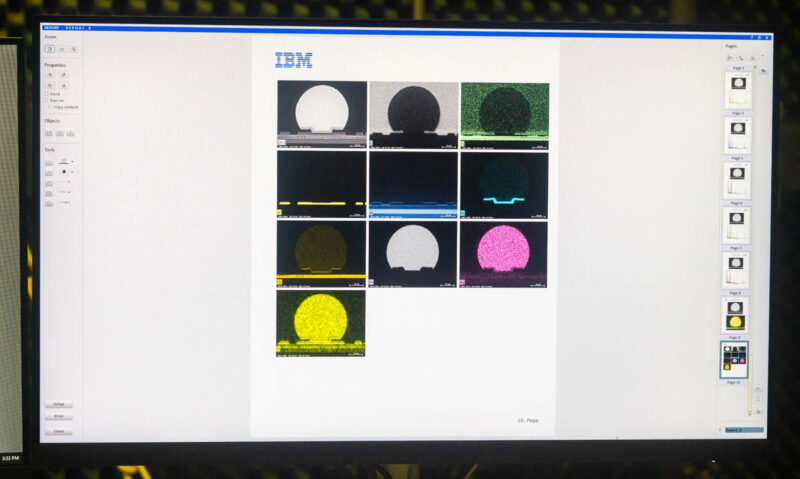
It was amazing to just see the scale of the operation. For example, here are solder balls.
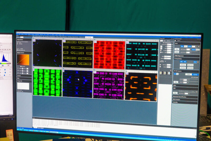
Here is the elemental analysis of where the elements are found around those balls.
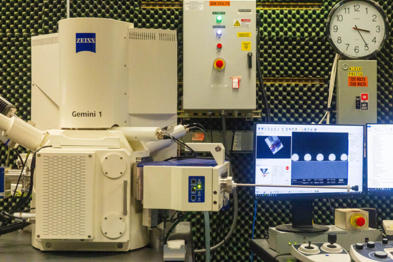
Once we got to the basement, we got to some of the wild machines that cost millions of dollars each and are so sensitive they can pick up windows being washed on the other side of the huge building.
These tools are for getting very deep into the materials. For example, IBM can see how metal layers interact at different depths inside chips.
Then there are the scanning tunneling microscopes that can see individual atoms.
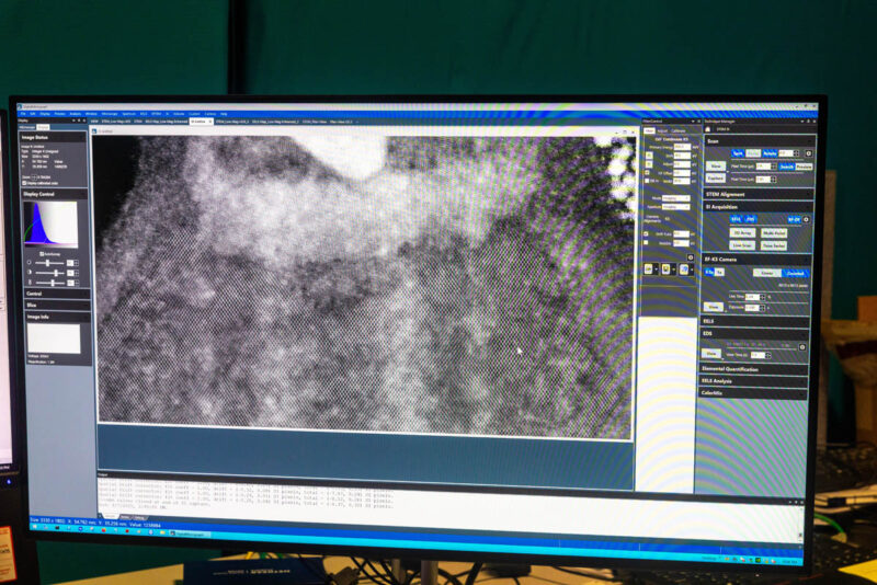
While in the above photo, it may look like we are getting a lot of artifacts from photographing a screen, most of that is actually different atoms. For example, the screen on the left in the photo below is full of silicon atoms.
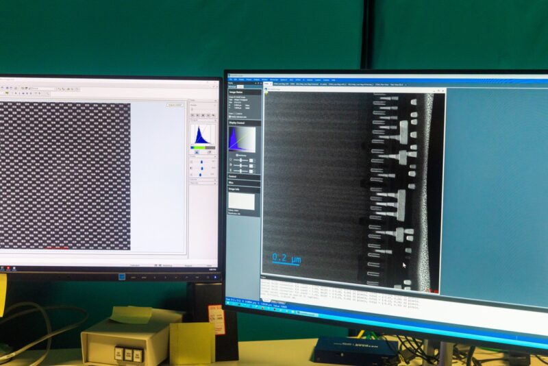
This type of analysis can be used to look at how the semiconductors are structured at a very low level since IBM is responsible for designing not just the z17 mainframe system, but all the way down to the Telum II CPU and Spyre AI accelerator silicon.
In the video we have more on these machines and even show some of the shock and shake machines that are in the lab.
Final Words
It was awesome to get to see not just the giant mainframe, but then see how IBM designs z17 all the way down to the individual atom for reliability. I have to say, when I issued the challenge that I wanted to see behind-the-scenes and how they make mainframes, I did not expect to be looking at a picture of a silicon atom structure on a screen.
The big thrust behind this is that there is far more that goes into making a mainframe beyond just putting off-the-shelf pieces together. Instead, IBM has to engineer the entire system from the raw materials to the software to process transactions reliably. I have been to a lot of cool places, and this is certainly one of the most interesting places I have seen in the industry.
If you want to learn more about IBM z17, you can do so here.


If you’re stuck on page 1 make sure you’re looking at page 2 since it gets way nerdier. Video is sooo cool too.
Thanks Tom. This was a fun one to do.
Wow, really cool and fascinating. The side profile cutaways remind me of the thermal conduction module cutaways IBM did for the 3080 and 3090 System/370 mainframes back in the 1980s. Those things were HUGE for that time – 1,800 pins in an interstitial staggered PGA with a pin pitch of 0.100″. They measured around 3 to 4 inches square and required chilled liquid cooling AND helium gas fill in the thermal hat to keep all that ECL in them happy. IBM continued to use TCM packaging right up to the POWER7 and System z/EC13. I have a POWER5+ MC-TCM in my chip collection as well as an earlier System/370 module out of a 4381 midsize mainframe system. These things are impossible to come by on eBay. You have to luck up on them. Thanks, Patrick. I appreciate posts like this one. :-)
What does one search for to find those x-ray machines for purchase second hand?
Also I spotted Patrick’s Easter egg: “bottom levt image”
IBM, still running the show at the top end of the spectrum. Excellent article, but still left hungry for more high-quality photos of the boards, the cooling tech, possibly a look at those CPU interconnect cables. Patrick your articles are becoming too short! Something like this deserves at least 4 for 5 pages! I appreciate the video-creation takes a lot of effort, I do hope to see more of big blue’s adventures in the future, I used to love their servers before the sale to Lenovo, always have a deep soft spot for them.
Most of the youngsters today have no idea of the part goliath’s such as IBM play behind the scenes. Just a shame they left the desktop scene all those years ago, would love to see a comeback to the consumer market, with their engineering prowess we could finally get to see some huge technology shifts in the mass market sectors, trend-setters they sure are.