
A few weeks ago, we showed the new IBM z17 Mainframe, which brings AI with Telum II and Spyre. I attended the launch, but the next day, I was able to tour IBM’s Fishkill facility, where they do engineering, including failure analysis. As part of that, we got some unique looks at hardware that few get to see.
There is a lot more in the video here:
We had to travel for this one, and we got special access. We need to say this is sponsored by IBM on anything we do related to that even if this was not a piece IBM asked us to do. It was, however, too cool for us to only have on video.
The New IBM z17 Telum II Processor
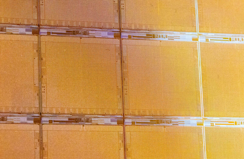
Something fun that we got to see during our visit to Fishkill is the IBM z17’s Telum II processor cut open for materials analysis. At the same time, IBM had a ton on display down to the wafers of Telum II processors.
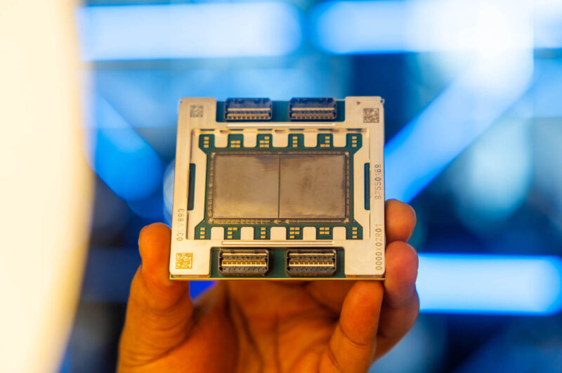
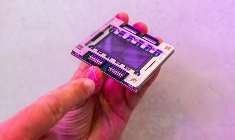
In our previous piece, we showed the dual chip modules or DCMs.
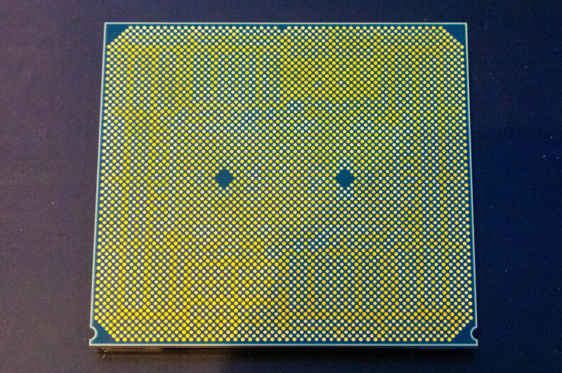
We also managed to grab a shot of the bottom pads.
The socket itself is neat. Instead of the I/O being completely through those bottom pads, there are also SMP cable connectors that aid in processor to processor communication.
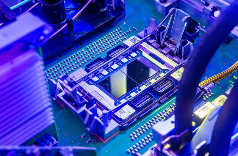
Here is another look at those.
Of course, this is just what we saw last time. I challenge IBM to show some behind-the-scenes of how these are made, and IBM let me into its Fishkill facility where we got down to the individual atom level. Let us get to that next.


If you’re stuck on page 1 make sure you’re looking at page 2 since it gets way nerdier. Video is sooo cool too.
Thanks Tom. This was a fun one to do.
Wow, really cool and fascinating. The side profile cutaways remind me of the thermal conduction module cutaways IBM did for the 3080 and 3090 System/370 mainframes back in the 1980s. Those things were HUGE for that time – 1,800 pins in an interstitial staggered PGA with a pin pitch of 0.100″. They measured around 3 to 4 inches square and required chilled liquid cooling AND helium gas fill in the thermal hat to keep all that ECL in them happy. IBM continued to use TCM packaging right up to the POWER7 and System z/EC13. I have a POWER5+ MC-TCM in my chip collection as well as an earlier System/370 module out of a 4381 midsize mainframe system. These things are impossible to come by on eBay. You have to luck up on them. Thanks, Patrick. I appreciate posts like this one. :-)
What does one search for to find those x-ray machines for purchase second hand?
Also I spotted Patrick’s Easter egg: “bottom levt image”
IBM, still running the show at the top end of the spectrum. Excellent article, but still left hungry for more high-quality photos of the boards, the cooling tech, possibly a look at those CPU interconnect cables. Patrick your articles are becoming too short! Something like this deserves at least 4 for 5 pages! I appreciate the video-creation takes a lot of effort, I do hope to see more of big blue’s adventures in the future, I used to love their servers before the sale to Lenovo, always have a deep soft spot for them.
Most of the youngsters today have no idea of the part goliath’s such as IBM play behind the scenes. Just a shame they left the desktop scene all those years ago, would love to see a comeback to the consumer market, with their engineering prowess we could finally get to see some huge technology shifts in the mass market sectors, trend-setters they sure are.