
Some days, I get to do very cool things. Today was one of those days as I was able to attend the IBM z17 Event where the newest IBM mainframe was launched. IBM flew me out and asked if I could write a LinkedIn article, so we have to say this is #sponsored as well I think. Still, I wanted to bring the content to our STH main site audience.
The IBM z17 Mainframe Brings AI with Telum II and Spyre
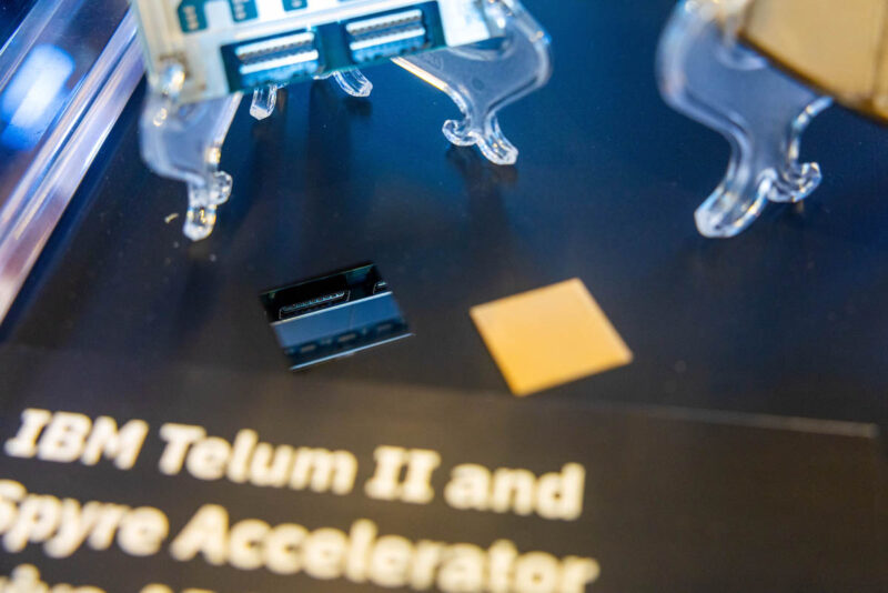
At the IBM z17 Event, the company announced its new Mainframe built around the new Telum II processor. We covered the processor at IBM Telum II Processor and Spyre AI Updates at Hot Chips 2024 so you can check that out for a bit more detail (or just IBM’s site.) Still, today, I got to see the processors in action and hold them.
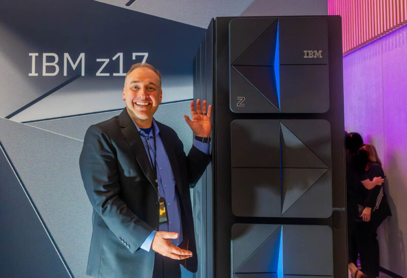
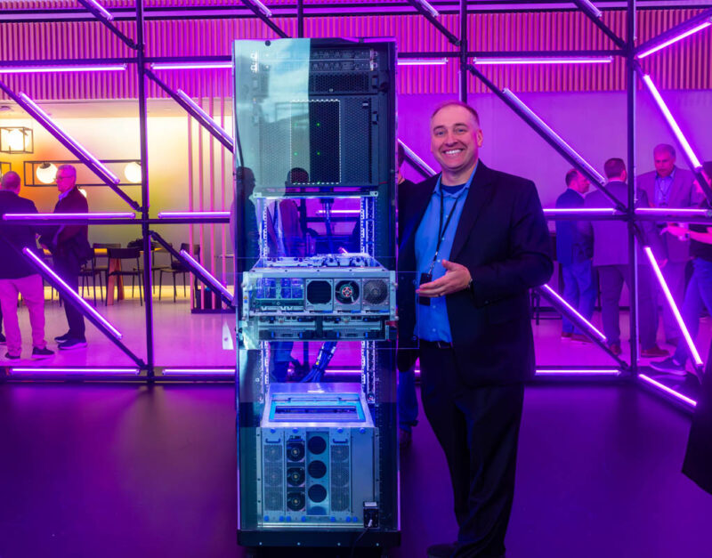
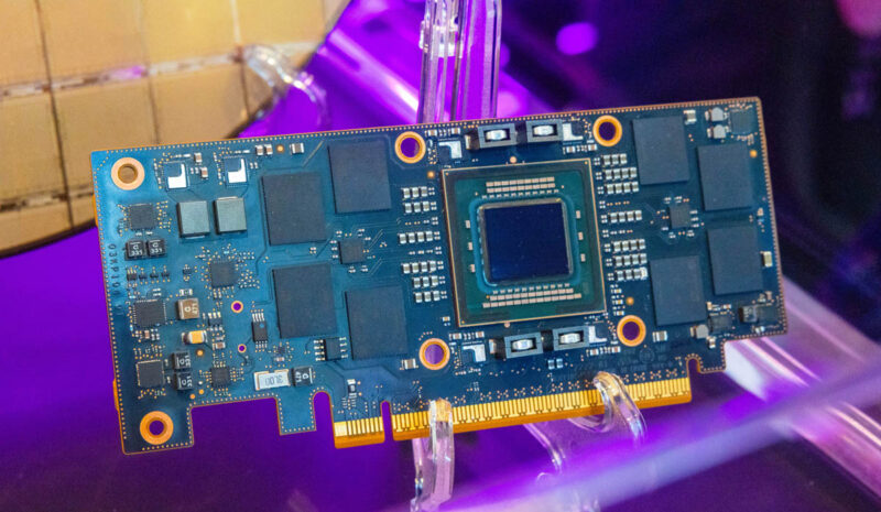
IBM had not just a z17 cabinet, but the one I spent more time with was the plexiglass clad demonstration unit with various components cutaway.
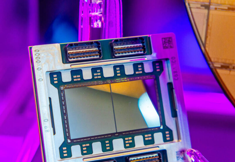
As a quick recap, the IBM Telum II is the newest generation of mainframe processor with features like larger caches and a new on-die AI accelerator implemented as a CISC instruction.
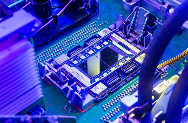
Since Will T just asked me as I was writing this what those connectors are on the sides, those are SMP connectors that allow this chip to be connected to the other chips in what can be up to a 32 processor system.
The entire setup is liquid cooled, and IBM is moving away from just distilled water to a new fluid for an easier lifetime of maintenance.
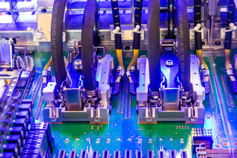
We have a better die shot on the LinkedIn article, but these liquid cooled sockets hold two Telum II dual chip modules.
Something I did not appreciate before today was that the motherboard in the system is very thick. I think I lost count at what looks like 40-50 layers. This cutaway is actually in the center of a forest of memory modules.
Here is one of the rear I/O expansion drawers at the rear. This is where the new Spyre AI accelerators go.
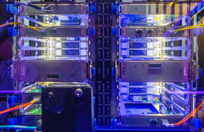
The IBM Spyre accelerators are 75W 128GB parts that are designed to be combined in sets of eight (up to I believe 48 per z17) for 1TB across eight accelerators.
The AI acceleration is important. Mainframes process the world’s financial data. There is an important task of performing fraud detection as close to real-time as possible. As bad actors use AI to commit fraud, more powerful AI driven algorithms are being developed to detect fraud which can have a significant ROI for these new systems.
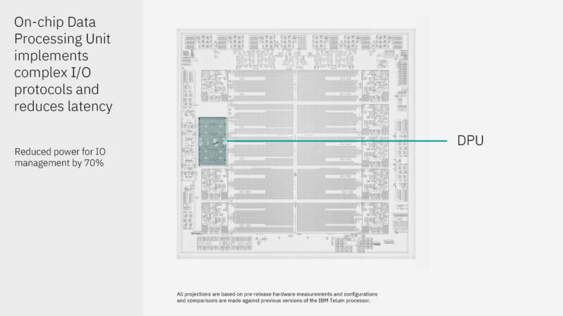
Moving data around the mainframe is a DPU. This helps offload the task of getting data to I/O or other parts of the system.
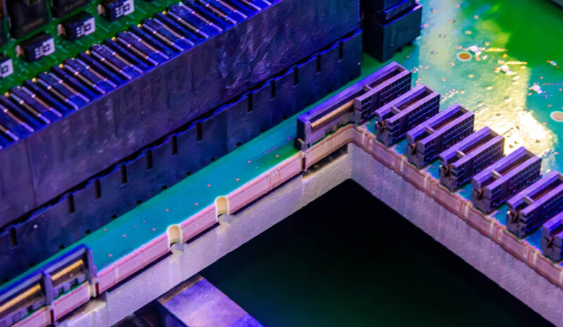
Something that we will get into more over the next few weeks is how all of these parts, down to using PCB over wires helps increase reliability of the system.
Final Words
Perhaps when folks think of many cores, lots of memory, liquid cooling, and AI their first instinct is not to dream of a mainframe. That is exactly what this is though. We have gotten requests to (and I have wanted to) look at a mainframe platform for some time. Stay tuned for the full video on STH coming later this month. I had the opportunity to spend today with IBM’s team going through the system, and will be getting some behind-the-scenes footage this week as well to show you what goes into this system. Given these are designed for highly sensitive transaction processing, some of the design decisions are very different. I know only a portion of our readers use mainframes, but there is some really cool technology here that I know STH’ers will enjoy.
- STH LinkedIn Post with more here.
- IBM z17 Page


A single z16 CPU has 8 cores, it would sure be great to get one CPU mounted on a motherboard (embedded) with a half dozen PCIe slots and 16 DIMM slots, all for less than U$20K; for home use.
Not to make it political, but it will be interesting to see if IBM and others like Unisys continue to have a business proposition over the long term if DOGE gets its way. There is often this notion that the large mainframes driving government operations are these warehouse size antiquated systems from the 1960s, when in fact, they are often modern Z-Series Mainframes that can run thousands of Linux VMs and other parallel systems at crazy scale for a very low TCO all while serving their transactional processing duties.
@haakebecks
If anything, DOGE is likely to push old (think before z12 old ..) mainframe kit to be replaced by these babies on an accelerated schedule.
The biggest waste is not in Z versus Midrange kit. There the TCO can easily go both ways, depending on the workload.
THE WASTE is running ancient Z series AND paying crazy amounts to keep them supported and maintained while the whole promise of the Z series is there is pretty much a full backwards compatibility guarantee ..
These are the best mainframe CPU photos ever taken. Fight me on that. IBM shoulda hired you to do its photos. Maybe they don’t because its a soul-less big ol’ company and these aren’t clean enough for their image. I’ve now saved that IBM Telum II In Socket Without Heatsink Close 1 as a desktop image for a Nvidia Jetson test system we’ve got. Too good.
I work at a bank, and we’ve got an entire team that just does Z and I’ve thought of them as Z for Zealots
@minosi… I personally don’t think so. Musk and crew are proponents of OTS or Semi Custom SOCs. Look no further than what Musk did with Grok. Threw oceans of money at Supermicro and they were on their way. None of these guys have experience with COBOL/ALGOL or even modern interpreters. Most of these folks are kids with no material enterprise experience and the “cloud” and microservices or containers solve everything. I do not see them going after a Z16/Z17 and leaning into the existing hardware and software ecosystem.