At Hot Chips 34, we got a look at the microarchitecture of Tesla Dojo. For those that do not know, Tesla is now consuming so many AI resources that not only does it have a giant NIVIDA GPU cluster, but it also is designing its own AI training infrastructure. At HC34, the company has two talks. This article is covering the microarchitecture, the next will cover the systems-level presentation.
Note: We are doing this piece live at HC34 during the presentation so please excuse typos.
Tesla Dojo AI System Microarchitecture at HC34
Tesla has its exascale AI-class system for machine learning. Basically, like its in-vehicle systems, Tesla has decided it has the scale to hire folks and build silicon and systems specifically for its application.
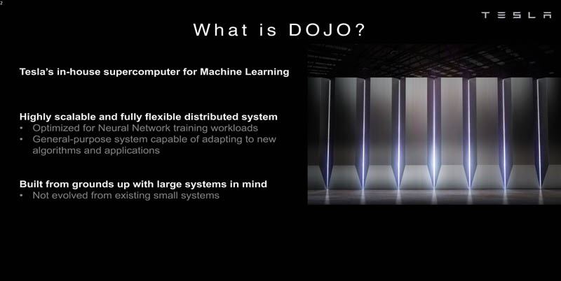
Tesla is looking at building the system from the ground up. It is not just building its own AI chips, it is building a supercomputer.
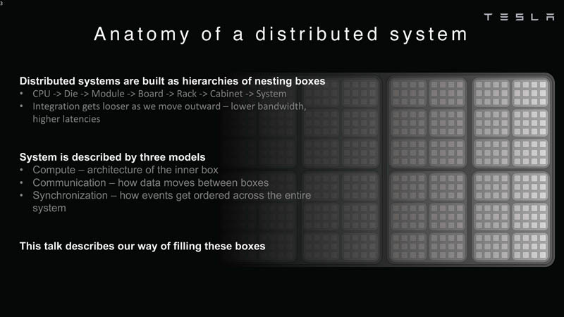
Each Dojo node has its own CPU, memory, and communication interface.
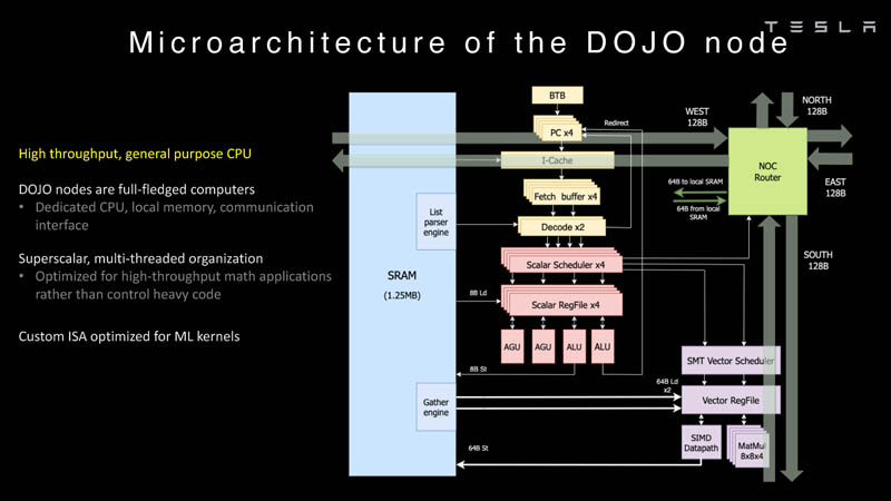
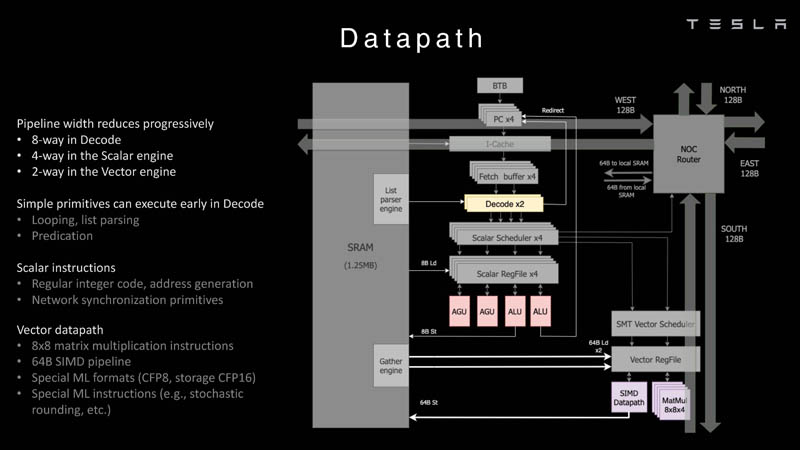
Here is the processing pipeline for Dojo’s processor.
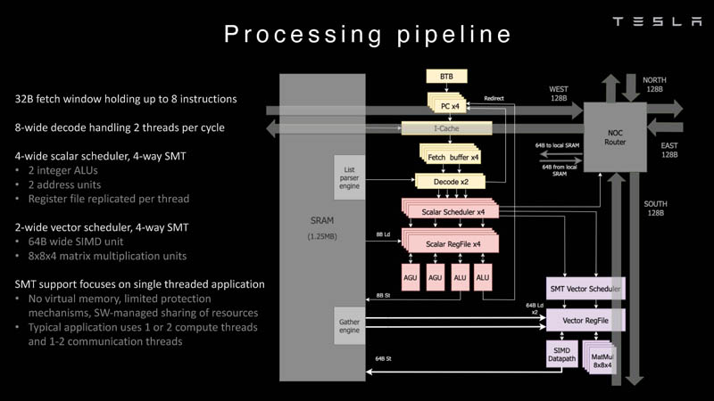
Each node has 1.25MB of SRAM. In AI training and inference chips, a common technique is to colocate memory with compute to minimize data transfer since the data transfer is very expensive from a power and performance perspective.
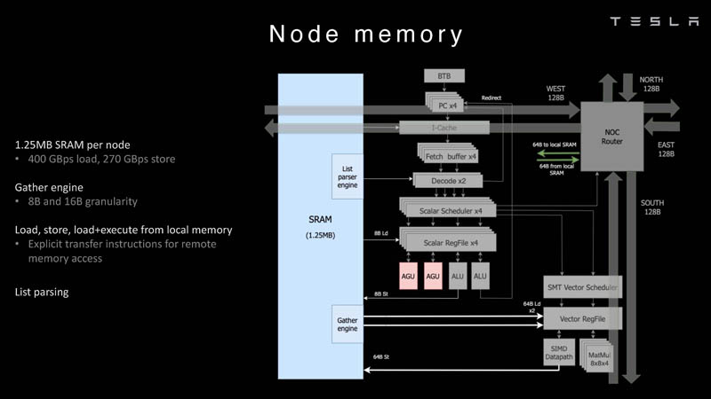
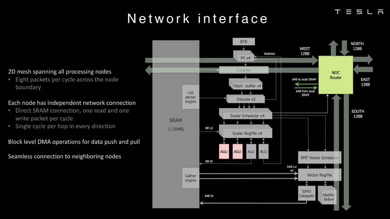
Each node then is connected to a 2D mesh.
Here is the data path overview:
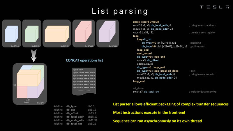
Here is an example of the list parsing that the chip can do.
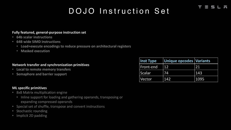
Here is more on the DOJO instruction set, this is Tesla’s creation and is not your typical Intel, Arm, NVIDIA, or AMD CPU/GPU’s instruction set.
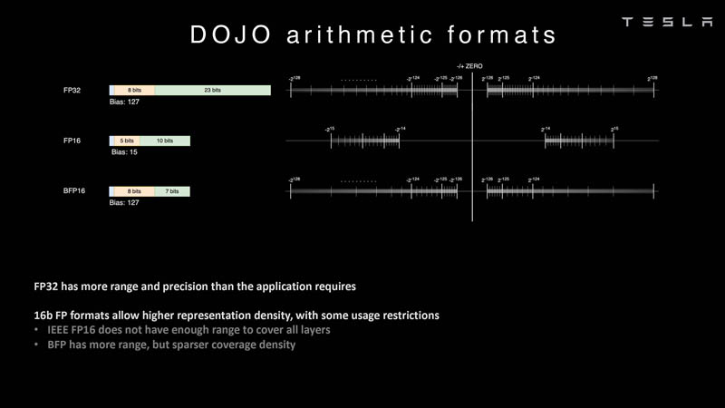
In AI, arithmetic formats are a big deal, and specifically which formats are supported by a chip. DOJO was an opportunity for Tesla to look at the formats commonly available such as FP32, FP16, and BFP16. These are common industry formats.
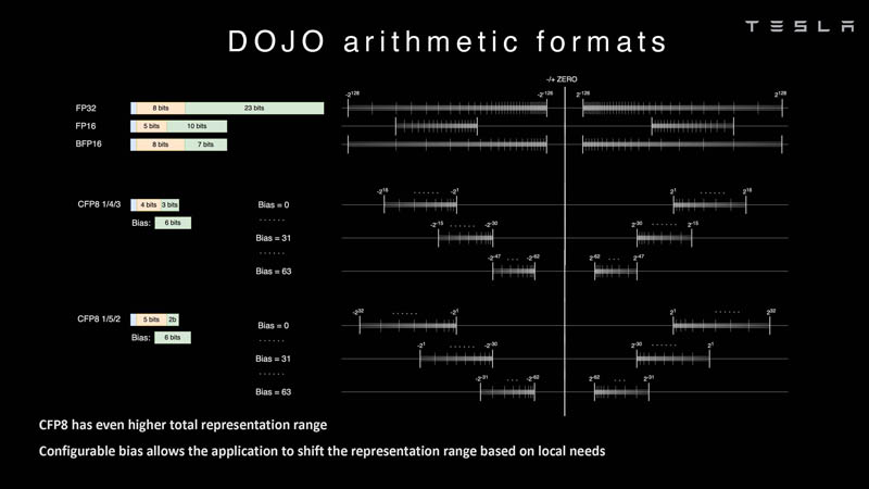
Tesla is also looking at configurable FP8 or CFP8. It has a 4/3 as well as a 5/2 range option. That is similar to what the NVIDIA H100 Hopper does with FP8. We also saw the Untether.AI Boqueria 1458 RISC-V Core AI Accelerator focus on different FP8 types.
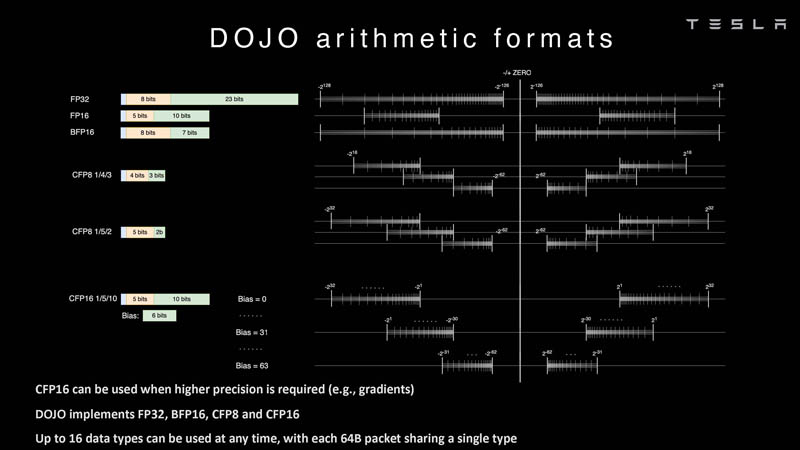
Tesla also has a different CFP16 format for higher precision. DOJO supports FP32, BFP16, CFP8, and CFP16.
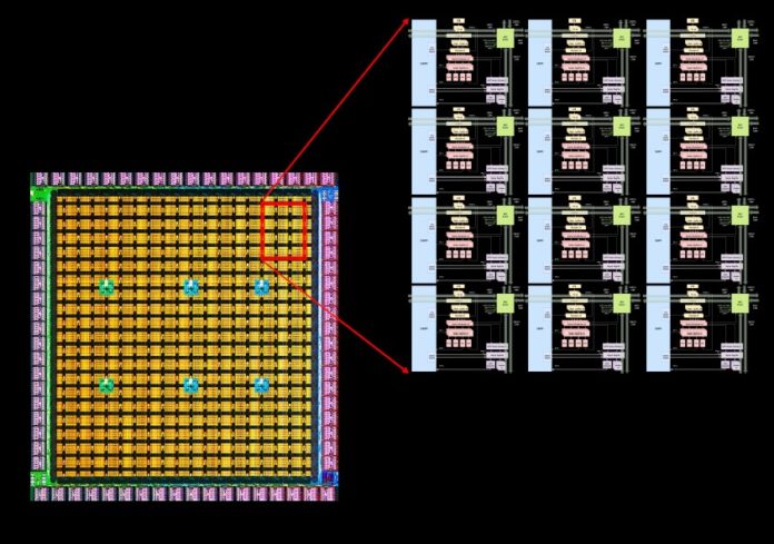
These cores are then integrated into a die that is manufactured. The Tesla D1 die is fabbed at TSMC on 7nm. Each chip has 354 DOJO processing nodes per die and 440MB of SRAM.
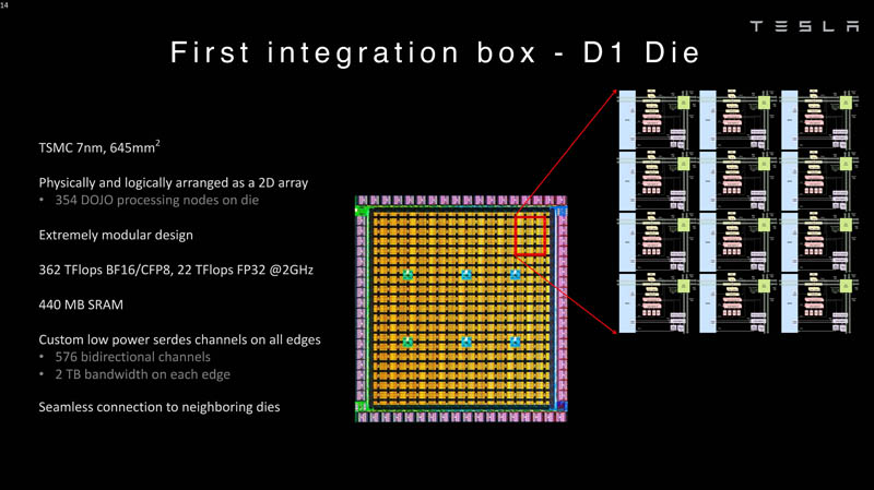
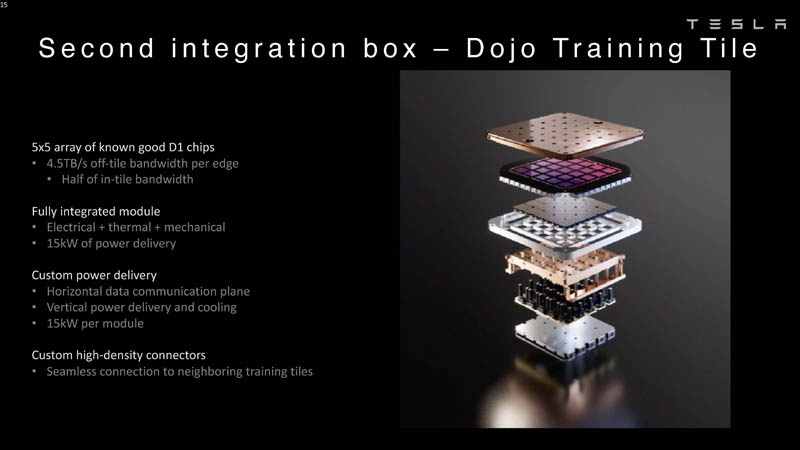
These D1 dies are packaged onto a Dojo Training Tile. The D1 chips are tested, then are assembled into a 5×5 tile. These tiles have 4.5TB/s of bandwidth per edge. They also have a 15kW power delivery envelope per module or roughly 600W per D1 chip minus whatever is used by the 40 I/O dies. The tile also includes all of the liquid cooling and mechanical packaging. This is conceptually similar to what Cerebras does packaging its WSE-2 giant chip. One can also see why something like the Lightmatter Passage would be attractive if a company did not want to design this.
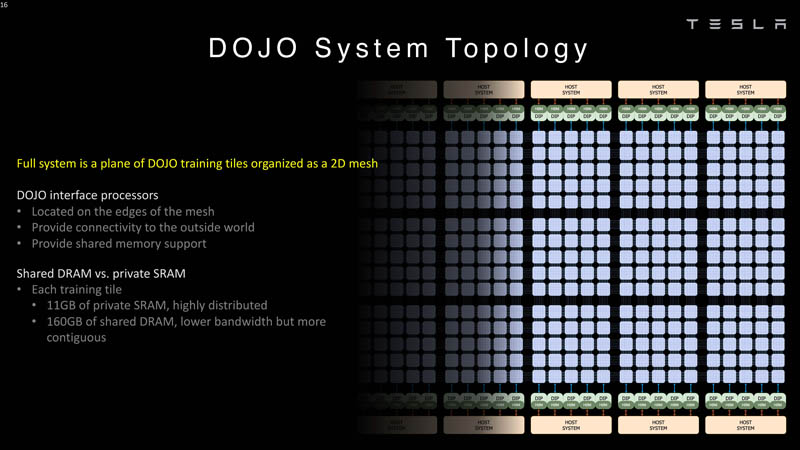
The DOJO interface processors are located on the edges of the 2D mesh. Each training tile has 11GB of SRAM and 160GB of shared DRAM.
Here are the bandwidth figures for the 2D mesh connecting the processing nodes.
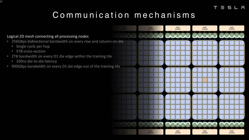
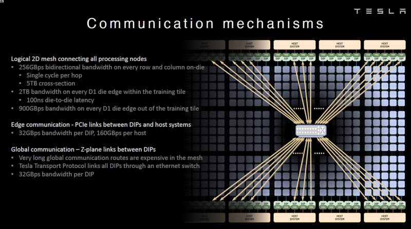
32GB/s links are available per DIP and host systems.
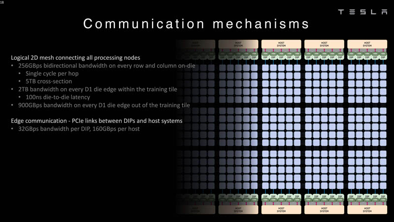
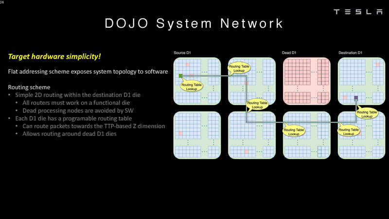
Tesla also has a Z-plane links for longer routes. In the next talk, Tesla talks about system-level innovation.
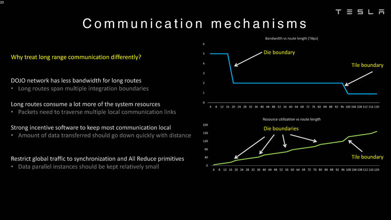
Here are latency boundaries to dies, and tiles and that is why they are treated differently in Dojo. The Z-plane links are needed because long routes are expensive.
Any processing node can access data across the system. Each node can push or pull data to SRAM or DRAM.
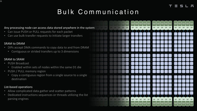
Tesla Dojo uses a flat addressing scheme for communication.
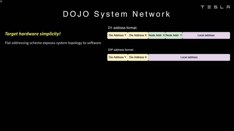
The chips can route around dead processing nodes in software.
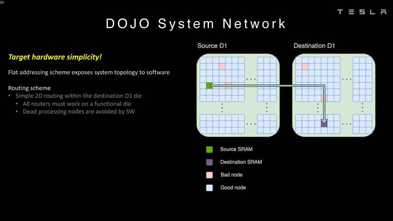
That means that software has to understand the system topology.
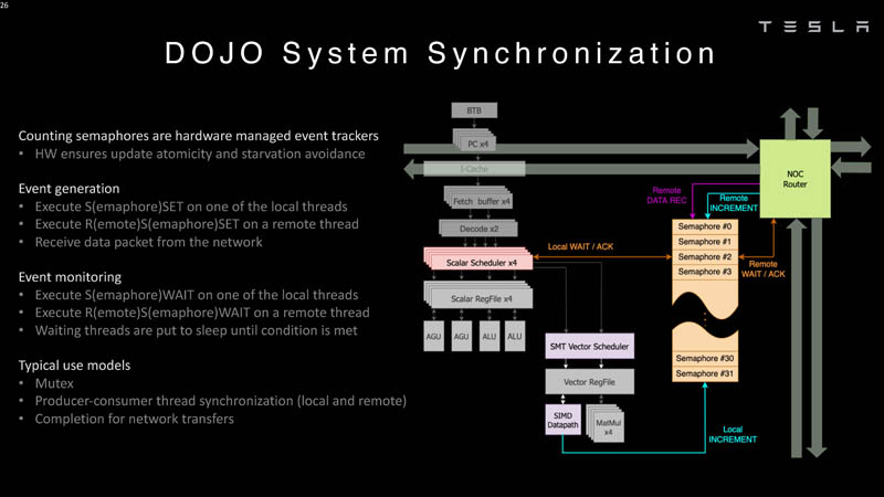
DOJO does not guarantee end-to-end traffic ordering so packets need to be counted at their destination.
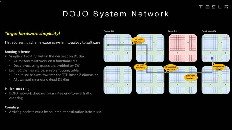
Here is how the packets are counted as part of the system synchronization.
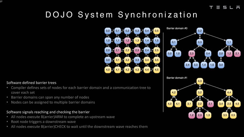
The compiler needs to define a tree with nodes.
Tesla says one exa-pod has more than 1 million CPUs (or compute nodes.) These are large-scale systems.
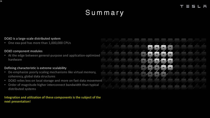
Tesla built Dojo specifically to work at a very large scale. Some startups look to build AI chips for one or a few chips per system. Tesla was focused on a much larger scale.
Final Words
In many ways, it makes sense that Tesla has a giant AI training farm. What is more exciting is that not only is it using commercially available systems, but it is also building its own chips and systems. Some of the ISA on the scalar side is borrowed from RISC-V but the vector side and a lot of the architecture Tesla made custom so this took a lot of work.
Next, we are going to take a look at the Dojo system level design. If this seemed too low level, the next talk is the one you may be looking for.

“Open the pod bay doors HAL”.