

SK hynix’s Hot Chips 2026 presentation is around high-bandwidth memory (HBM) and advanced packaging. From a slide flip, it looks like they will be covering the 3D stacking, bonding, and system integration choices behind high-bandwidth memory.
Like the others, we are doing these live, so please excuse typos.
SK hynix HBM Packaging at Hot Chips 2026
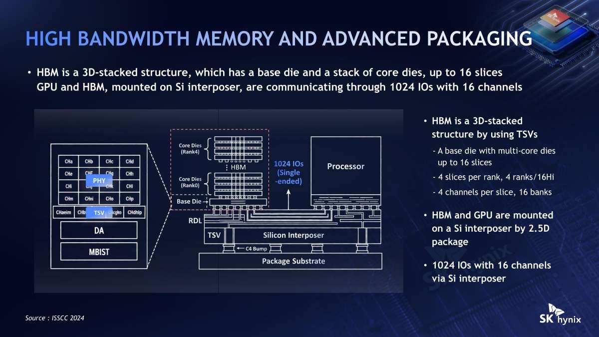
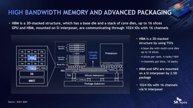
SK hynix began by explaining that HBM is a 3D-stacked structure comprising a base die and a stack of core dies, up to 16 slices in total. GPU and HBM sit together on a silicon interposer in a 2.5D package and communicate via 1024 IOs across 16 channels, with four slices per rank and four ranks in a 16-high stack. Getting that interposer connection right matters because it is where HBM meets the accelerator.
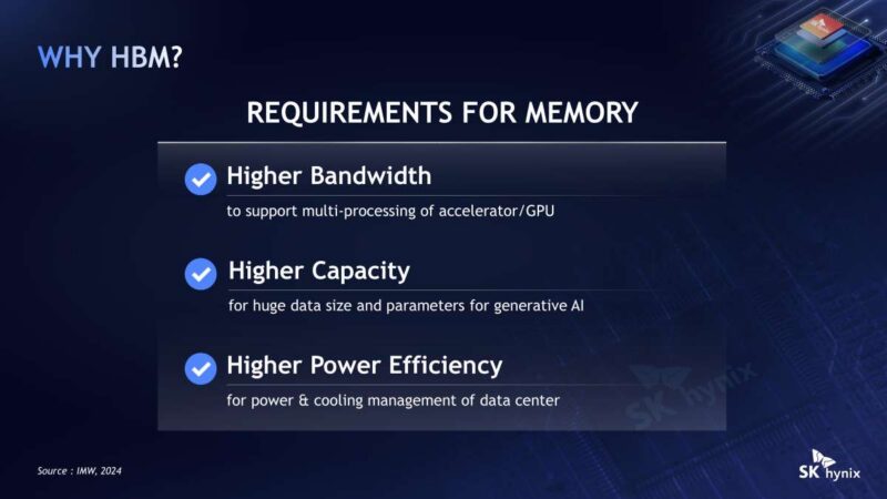
Higher bandwidth, higher capacity, and higher power efficiency are the why behind advancing HBM.
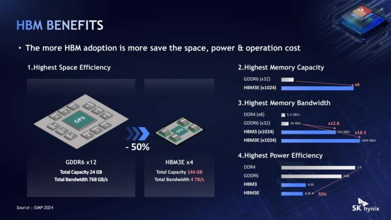
Despite the per-GB cost being higher for HBM, SK hynix argues that wider HBM adoption saves space, power, and operating costs. This is a bit of an interesting comparison, but it is showing 12x GDDR6 sites versus 4x HBM3E sites as being more space efficient while providing more bandwidth and capacity. This seems like a bit of an odd direct comparison point since cards like the consumer(-ish) NVIDIA GeForce RTX 5090 have 32GB of GDDR7, but OK.
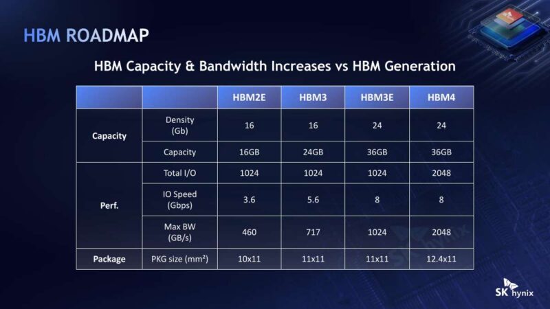
Capacity and bandwidth climb with every HBM generation. HBM2E delivered 460 GB/s, HBM3 moved to 717 GB/s, HBM3E reached 1024 GB/s, and HBM4 doubles the picture with 2048 GB/s across 2048 IOs. Package size grows too, from a 10×11 mm base to a 12.4×11 mm footprint on HBM4.
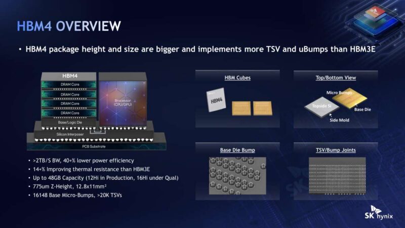
HBM4 has more TSVs and micro-bumps. SK hynix lists over 20K TSVs and 16148 base micro-bumps on a 12.8×11 mm part with a 775 um Z-height, targeting more than 2 TB/s of bandwidth with a 40+ percent power-efficiency gain and improved thermal resistance. Capacity climbs to 48 GB, with 12-high in production and 16-high under qualification.
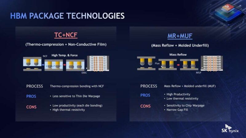
Stacking die-to-die has two main bonding choices, and SK hynix lays out the trade-off between thermo-compression bonding with non-conductive film and mass reflow with molded underfill. TC+NCF offers high productivity and low thermal resistivity but is sensitive to chip warpage, while MR+MUF handles thin-die warpage better at the cost of higher thermal resistivity and a narrower gap-fill window. Choosing between them shapes downstream yield and thermal behavior.
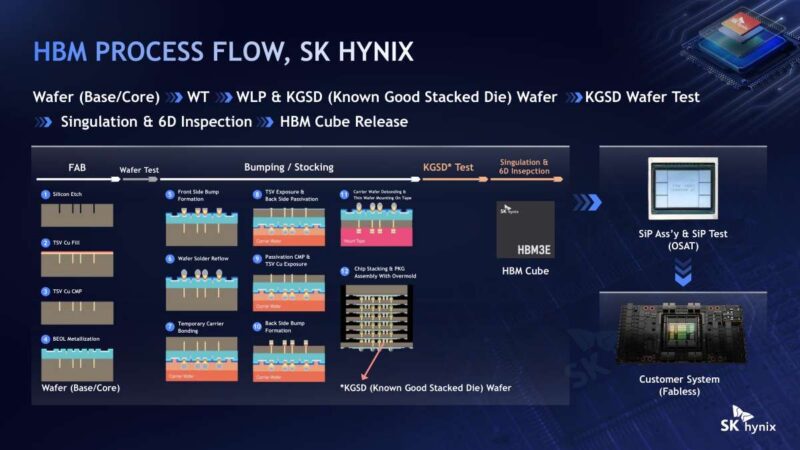
SK hynix runs a full wafer-level flow behind HBM assembly, from silicon etch and TSV copper fill through BEOL metallization, wafer thinning, back-side processing, singulation, and testing. A known-good stacked die (KGSD) wafer step allows SK hynix to test each cube before it reaches system-level packaging, preventing defective units from consuming costly interposer real estate.
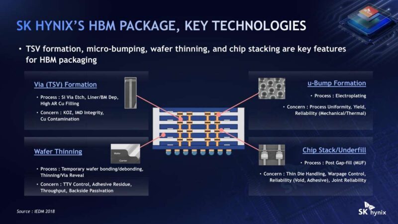
TSV formation, micro-bumping, wafer thinning, and chip stacking carry most of the HBM packaging challenge. SK hynix flags process uniformity, yield, and copper contamination as concerns on the TSV and bump side, then points to thin-die handling and warpage control during wafer thinning and stack assembly with underfill.
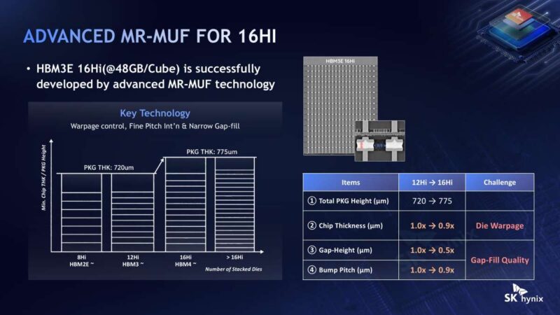
The HBM3E 16-high part at 48GB per cube marks a packaging milestone, since adding two more die on top of the earlier 12-high stack forces the package to stay inside the same Z-height budget. SK hynix had to cut chip thickness, gap height, and bump pitch roughly in half to fit the taller stack while keeping gap-fill quality intact.
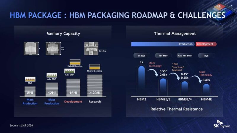
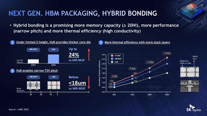
As stack height rises toward 20 or more die, thermal management becomes the binding constraint. This figure compares relative thermal resistance across bonding and material-stack options, from plain molded underfill through advanced MR-MUF and hybrid bonding, with each step reducing thermal resistance while supporting more layers.
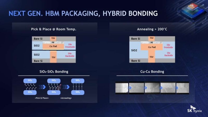
Hybrid bonding changes how a stack gets assembled. Pick and place occurs at room temperature, and an anneal above 200C forms SiO2-to-SiO2 and Cu-to-Cu bonds, which is the mechanism that enables the stack to shed the bumps and gap-fill of older approaches.
SK hynix positions hybrid bonding as the path to 20-or-more-high stacks, wider performance from a narrower bump pitch, and better thermal efficiency through higher conductivity. At a fixed Z-height, hybrid bonding allows the die to use a thicker core and pushes bump pitch below 18 um, which MR-MUF cannot manage.
SK hynix compared its approach with competitor cooling schemes. Its i-HBM embeds a high-thermal-conductivity, electrically insulating cooling component within the hot die-to-die PHY area to create a dedicated heat path, targeting a reduction in thermal resistance of over 30 percent. Samsung HPB moves DRAM next to the processor with a copper heat spreader, and Micron refines the base-die circuit design for efficiency.
![SK hynix [SK hynix i-HBM]](https://www.servethehome.com/wp-content/uploads/2026/08/sk-hynix-hbm-packaging-slide-15-800x450.jpg)
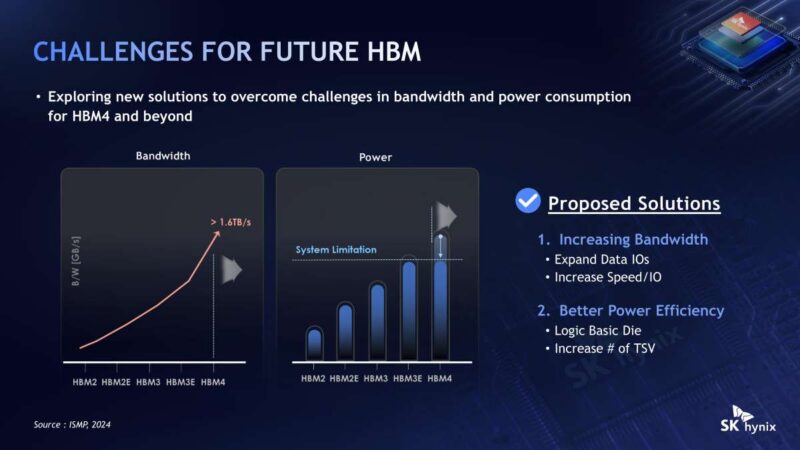
Bandwidth growth comes from pushing more data IOs and a faster I/O rate, with logic process integration in the picture. SK hynix shows per-unit bandwidth climbing from 0.5 TB/s on HBM2E to 2.0 TB/s on HBM4, with the HBM3E-to-HBM4 step doubling I/O speed while the data-IO count moves past 1K.

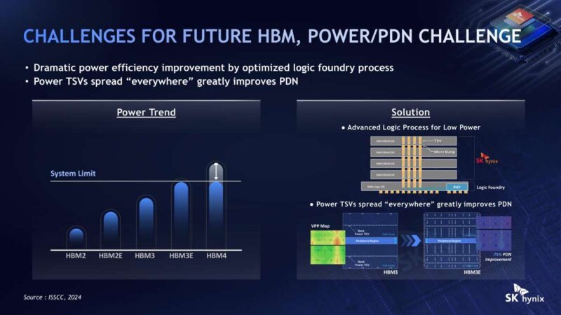
On the power side, SK hynix leans on an optimized logic foundry process and power TSVs spread across the part to improve the power delivery network. SK hynix highlights a 75 percent PDN improvement across recent HBM generations as the low-power logic approach keeps scaling.
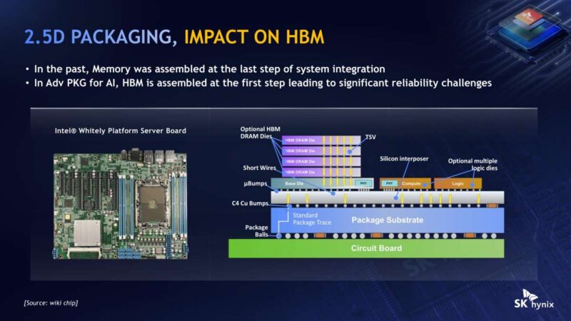
SK hynix then shifts to system-level impact, noting that memory used to be assembled last in the system integration flow. In advanced packaging for AI, HBM is now assembled first, which puts the cubes and the interposer under much stronger reliability pressure before the rest of the package is built. The photo is a pretty old motherboard which is fun.
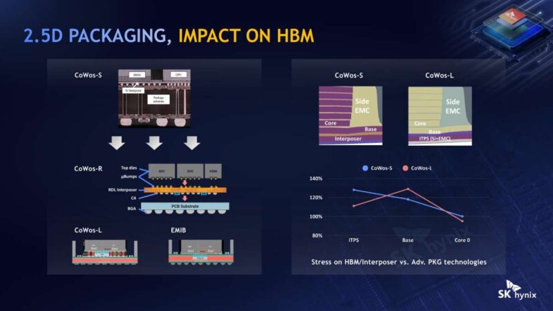
SK hynix is now comparing the major advanced packaging approaches, including CoWoS-S, CoWoS-L, and EMIB, and where each puts stress on the HBM cubes and the silicon interposer. Packaging choice changes how much mechanical and thermal stress the HBM stack must absorb.
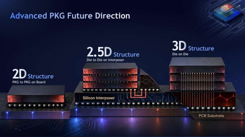
Finally, there are three packaging direction tiers, from die-on-die to die-to-die on an interposer to package-to-package on a board. Placing HBM in that hierarchy shows why it sits in the most demanding tier and why SK hynix is pushing so hard on stacking and bonding.
It feels like SK hynix is focusing on packaging a lot here compared to some of the other HBM talks at Hot Chips.
Final Words
SK hynix’s Hot Chips 2026 presentation made it clear that HBM packaging is tightening into a co-design problem in which bonding, thermal, and interposer stress all interact. I wish the company had gone more into some of the custom HBM solutions or even HBM5 in their talk, but this is what we got. Hopefully we will get more information on those soon-ish.
We have a full recap on the Substack, including where all of these pieces ranked in terms of popularity:



Okay, great, lots of RAM for AI data centers. What about reasonably priced RAM for the little people?