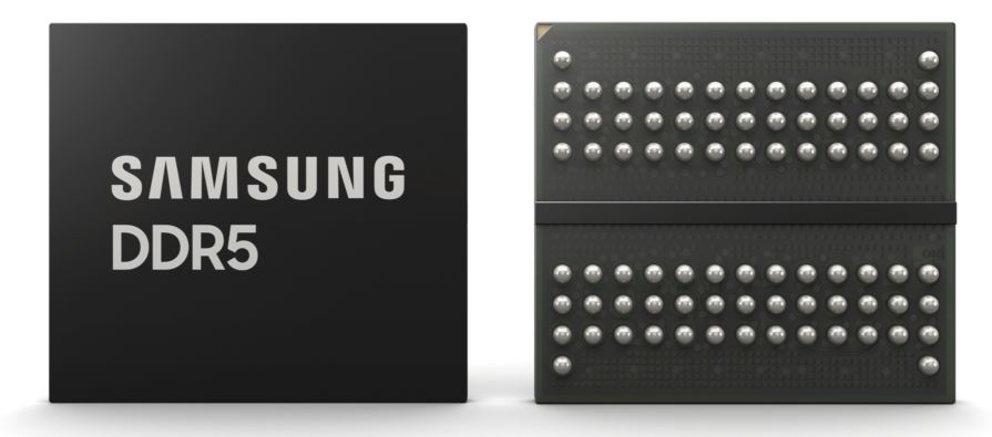
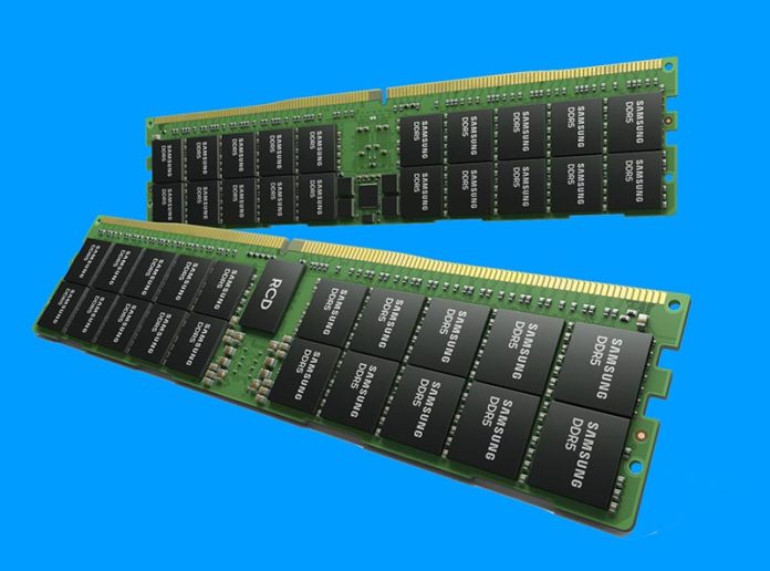
In the semiconductor manufacturing industry, extreme ultraviolet lithography (EUV) is a major advancement that we are going to see more of. Samsung announced that it started using EUV in its memory products in early 2020, and it is now up to five EUV layers for its DDR5 production.
Samsung DDR5 Uses EUV at 14nm
Aside from the use of EUV, the other big advancement is that Samsung is making its DDR5 now at 14nm. Samsung says that drives better wafer efficiency, or the ability to have more GB of DRAM come off of each wafer. Samsung says the process improvements mean it is getting around 20% better wafer productivity as a result. It also is said to lower the overall power consumption of the new DDR5 modules by up to 20% compared to the previous generation.

In terms of speed, Samsung says that its 14nm DRAM will bring speeds to 7.2Gbps. This is largely due to the DDR5 over DDR4 generational change. The net impact is more than twice the bandwidth.
Final Words
Overall, this is a evolutionary step in the industry. We are just on the cusp of the transition from DDR4 to DDR5. As a result, Samsung, and other manufacturers are looking at ramping production beyond the initial production that has been taking place to enable the next-generation chip launches. As such, these manufacturers are also looking at the more modern manufacturing technologies.
What is also clear is that memory is becoming a more important focus for the industry, and specifically how memory can be better utilized. We just had a story about VMware Project Capitola. That effort is really one designed to drive lower data center costs by decreasing the stranded RAM in servers. We have also seen major initiatives by hyper-scalers and also with the upcoming CXL 2.0 constructs to manage the memory footprint growth in servers. DDR5 currently has a steep price premium over DDR4 and at server scale deployments so driving efficiency to help offset the costs of the technology transitions will hopefully start the industry down the curve of more mainstream pricing.


