Pensando presented its Distributed Services Architecture (DSA) at Hot Chips 32 (2020.) Many of our readers will wonder what a DSA is. The closest analogy we can use is that it is a SmartNIC. Pensando has some different flavor to what they are doing, but that is the basic thrust of the solution when one looks beyond the basics.
Pensando Distributed Services Architecture Solution
Pensando has a PCIe device that provides many network features along with storage analytics. If you look at the way Pensando describes DSA, it covers a lot of the functionality we see in other SmartNIC solutions.
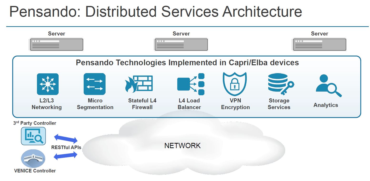
Instead of using an off-the-shelf FPGA, Pensando has its own chips specifically designed for this functionality. The networking path is largely based on P4 programmable pipelines and Pensando is heavily invested in P4 being the edge networking paradigm. If you want to draw some parallels, the Intel Tofino2 Next-Gen Programmable Switch also uses P4.
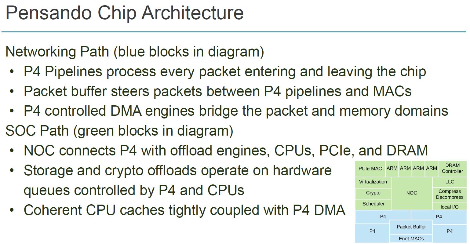
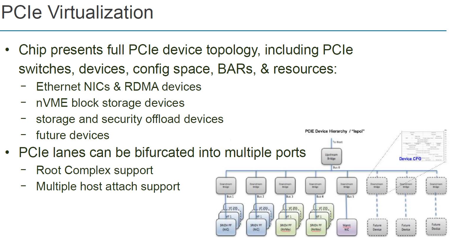
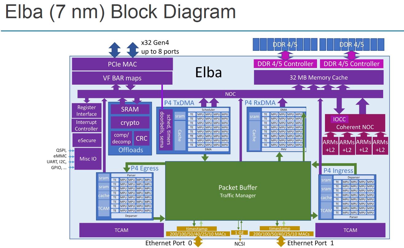
The chip itself has a number of different functions. It has a network on chip that connects PCIe, networking pipelines, compression, crypto, DRAM, and even Arm compute complexes. Instead of going into the P4 programmable pipelines, we are going to focus on the other features. First, the chip itself is presented on a PCIe bus to a server. It can present an Ethernet NIC, NVMe storage, and other functions. Beyond that, the PCIe lanes can connect to other devices. As an example, one could present a PCIe root complex and attach to NVMe drives directly or connect to multiple hosts, e.g. Facebook Yosemite platforms.
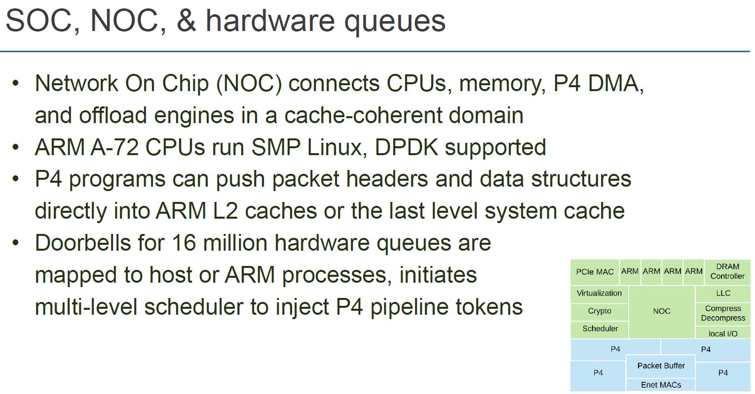
The chip has its own network on chip as well as a complex of Arm A72 cores. We were told that these run Yocto Linux. Linux is, by far, the most common OS for SmartNICs.
Since these are designed for cloud and next-gen enterprise workloads, we have security features such as secure boot and a root of trust. We also have crypto offload engines as this is an area that software support for NIC offload is very mature already.
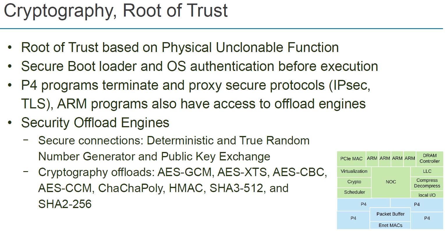
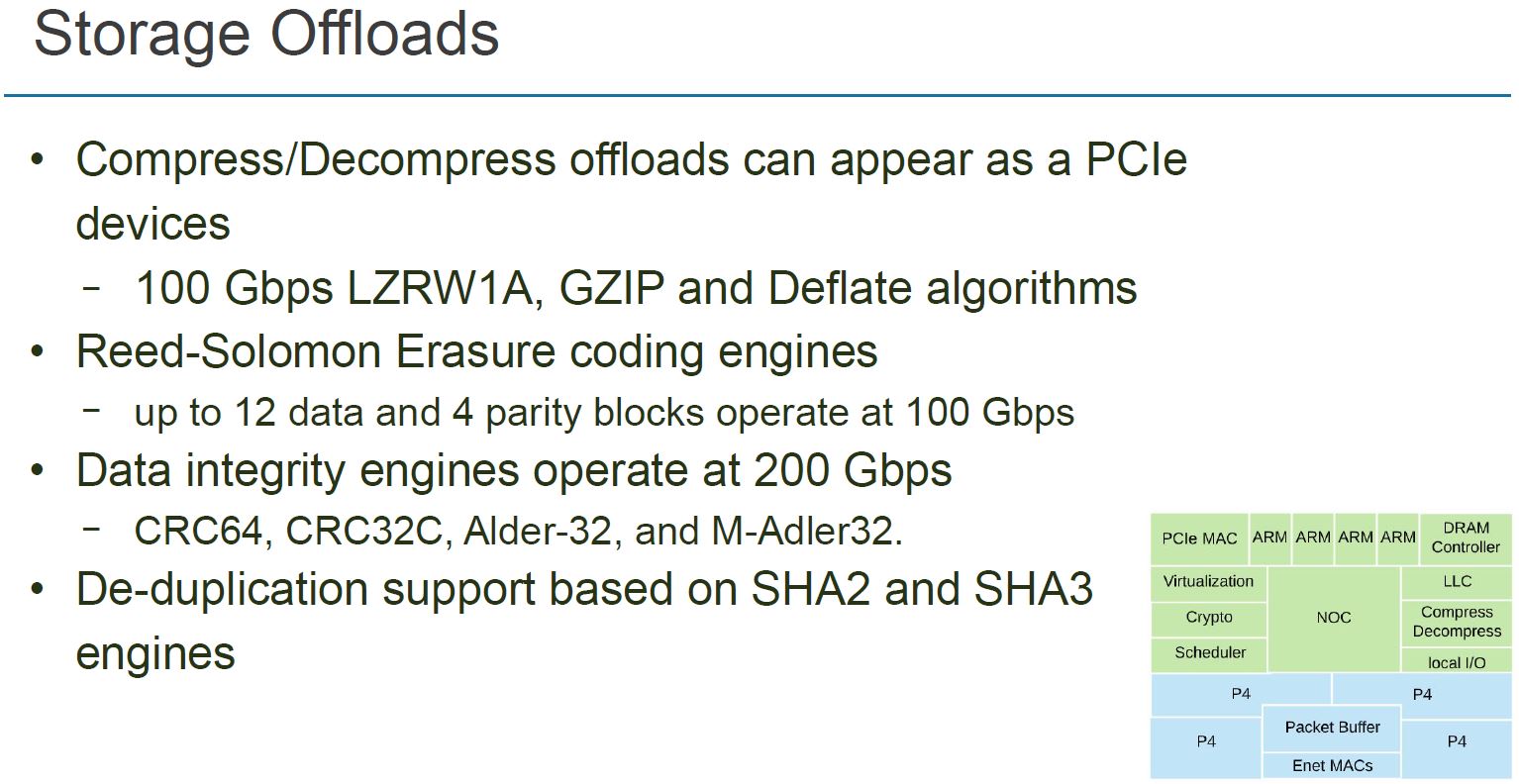
Aside from the networking side, we also have storage acceleration. There is compression/ decompression onboard. The solution can also do erasure coding (think more modern RAID) for storage taking that workload from the CPU.
Overall, this is a well-designed solution. There is more on the P4 side, but we wanted to focus on the parts outside of that since our audience is primarily those that build and deploy server systems rather than P4 programmers.
Pensando Capri and Elba Chips
On the chips themselves, Pensando has two. The Capri is the company’s first-generation part. The next-generation Elba part is in a prototype stage now. Here you can see some basic specs and comparisons.
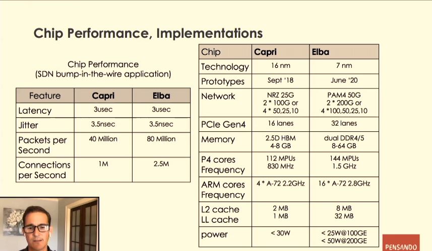
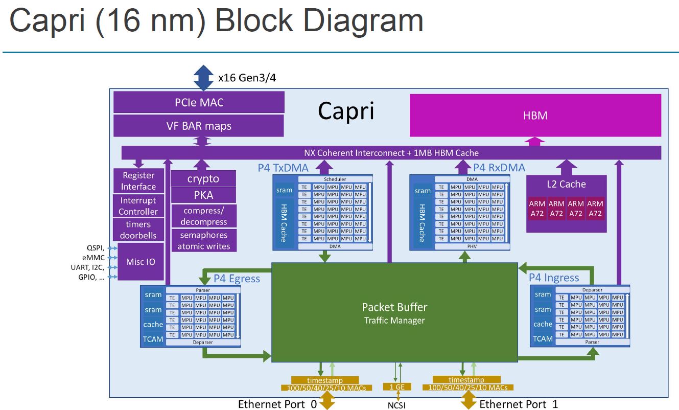
The Pensando Capri chip had HBM memory and was built on a 16nm process. We see this more as a V1 offering that was later iterated on in Elba.
Elba is the newer part. It is built on 7nm and has 16 Arm cores. Everything is upgraded included the networking and PCIe Gen4 connectivity.
With Elba, Pensando switched from HBM to DDR4/5 because it wanted to increase memory capacity. DDR is deployment is more flexible and HBM needs to be set up front with the ASIC. Also, the company moved from using memory as much to relying more on SRAM. DDR is also less expensive than HBM. Overall, the switch meant that it made sense to move to slower but larger memory.
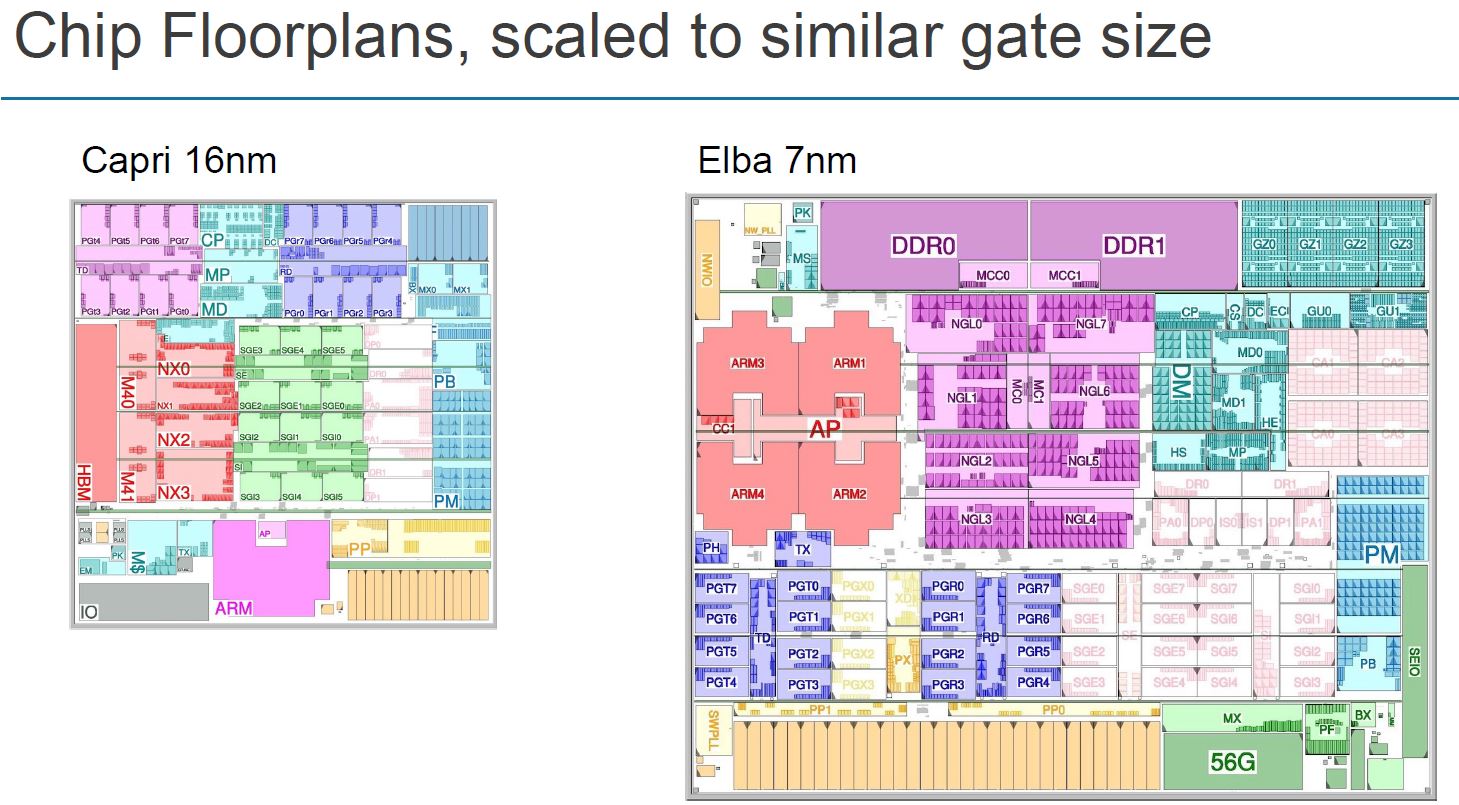
Since this is the week of Hot Chips, we wanted to point out just how much die area the DDR controllers take up. We covered this earlier this week in our IBM POWER10 Searching for the Holy Grail of Compute in the context of why IBM moved to OMI since it frees up die area. In a design like this, it is not necessarily required, but it is a good illustration of just how much die area is required for DDR4 controllers these days.
Final Words
Overall, the Pensando solution is very interesting. At the same time, it seems to be a bit further off. We have not had either Pensando, nor a storage/ networking/ server vendor ask us to review a Pensando equipped server at this point so it is hard to give an evaluation as we would in one of our hands-on reviews. Still, we are working to get more SmartNIC content on STH since we know this will be an area of interest in the future for STH readers.

I just want to know physically how they interface with 32 lanes of PCIe.
Another great article from you Patrick, was hoping you could cover the P4 part in terms of hardware implementation and use cases in another post.