
PCI-SIG announced that the PCIe 8.0 specification draft 0.5 is now available to members, marking the completion of the first official draft ahead of schedule. The full PCIe 8.0 specification remains on track for release by 2028, delivering 256GT/s raw transfer rates and up to 1.0TB/s in bi-directional bandwidth for a x16 configuration.
PCI-SIG PCIe 8.0 Update
This is the next step after the PCIe 8.0 announcement by the PCI-SIG that we covered previously. Draft 0.5 incorporates member feedback from the draft 0.3 specification that arrived in September 2025, and PCI-SIG says the standard remains on track for a full specification release in 2028.
PCI-SIG’s headline slide shows the basic target: PCIe 8.0 doubles PCIe 7.0 from 128 GT/s to 256 GT/s while keeping PAM4 signaling and FLIT encoding.
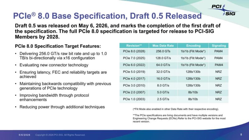
The generational roadmap is important because PCIe 7.0 was just released to members in June 2025. PCIe 8.0 is not a near-term platform feature, but the 2028 target tells silicon, connector, retimer vendors, and platform teams where future versions of the interconnect standard are headed.
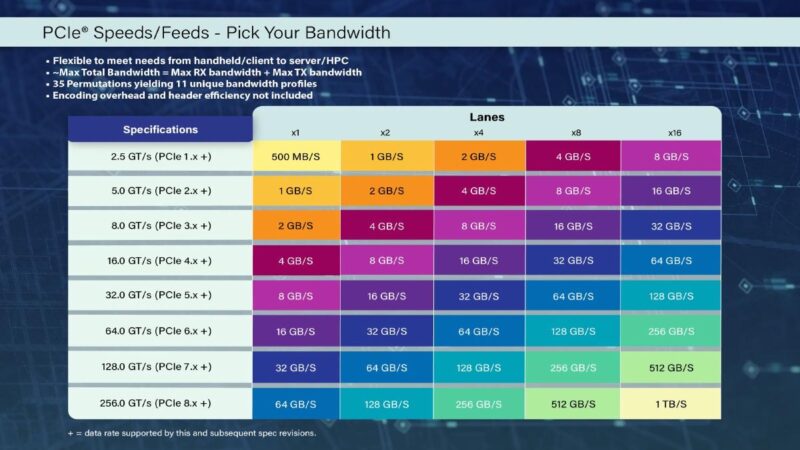
One useful way to frame the update is in terms of lane bandwidth. PCI-SIG’s bandwidth table shows PCIe 8.0 moving a x16 link to 1TB/s, while even a x4 link reaches 256GB/s. That is a lot of I/O bandwidth for future accelerators, NICs, SSDs, and CXL-adjacent platform designs. This is always one of the most useful charts to keep handy if you have to calculate or reference PCIe speeds often.
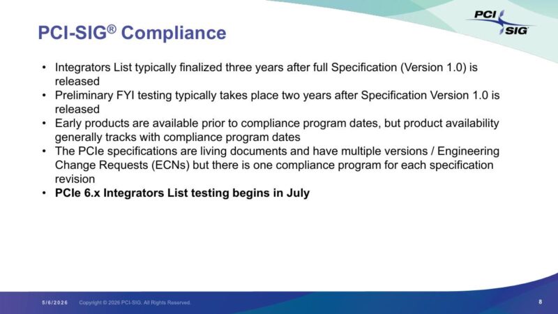
Compliance timing usually trails the final specification. PCI-SIG says integrator lists are typically finalized three years after a full specification release, with preliminary testing usually starting two years after version 1.0. Early products can arrive before formal compliance, but the compliance program makes broader ecosystem interoperability easier.
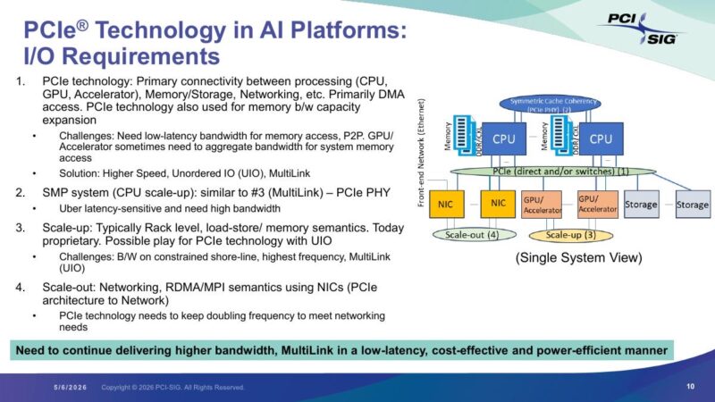
AI platforms are one of the obvious pressure points. PCIe remains the primary I/O fabric between CPUs, GPUs, accelerators, memory expansion, storage, and networking devices. As accelerator platforms grow, PCI-SIG points to higher speeds, unordered I/O, and MultiLink work as part of the broader bandwidth and latency story.
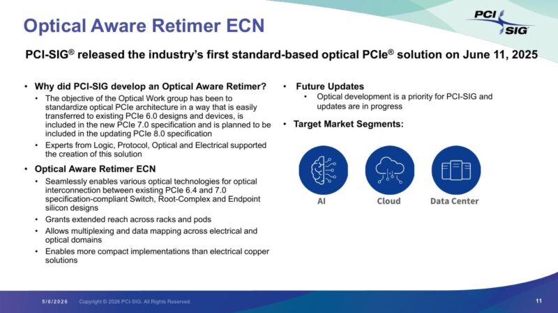
Electrical reach gets harder as signaling speeds rise, so optical PCIe work is becoming more relevant. PCI-SIG released an Optical Aware Retimer ECN in June 2025 for PCIe 6.0 and 7.0 compliant designs, with optical updates planned for PCIe 8.0. There is a reason we have been seeing demos like the Microchip PCIe Gen5 x16 over QSFP56-DD and Kioxia AIO Core and Kyocera Develop PCIe Gen5 Over Optics SSD.
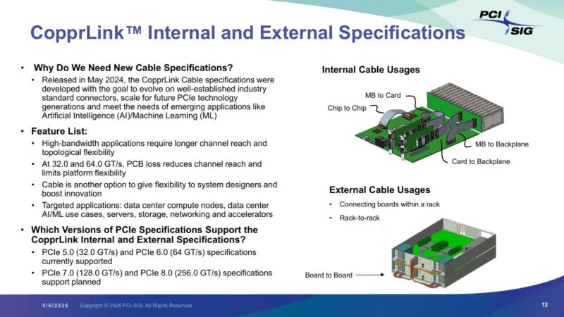
Copper cabling is another part of the platform story. The CopprLink internal and external specifications currently support PCIe 5.0 and PCIe 6.0, with support for PCIe 7.0 and PCIe 8.0 planned. That matters because future systems will need more topology flexibility than short motherboard traces alone can provide.
Still lots of activity around next-generation PCIe.
Final Words
PCIe 8.0 draft 0.5 represents steady progress in the I/O interconnect space as AI and data center workloads demand ever-higher bandwidth. The 2028 target for full release gives silicon vendors time to develop compliant products once the specification finalizes. Optical and copper cable work running alongside the base spec should help system designers manage signal integrity and overcome reach challenges. That is an absolute ton of bandwidth per lane, which also just gets us excited for the future generations of servers.


Seems like the spec is probably closer to “aspirational” at this point, since we have very limited PCIE6 usage and zero PCIE7 usage yet. When do we switch to optical interconnects again?
The spec is supposed to be ~3 years behind PCIe 7, so it’s not *that* close yet. PCIe 6 is running late, but it sounds like most of the pieces are available *except* for CPUs from Intel or AMD.
I’d love to see optical as a first-class reasonably-priced replacement for MCIO, but I have a hard time seeing cheap 16-lane optics at 256 Gbps per lane as a thing any time in the near future. I have this mental model of a tiny little motherboard with CPU+RAM SoC, a handful of back-panel ports, and a bunch of singlemode LC connectors that can be cabled up to slots, NVMe backplanes, CXL RAM, external CXL switches, or whatever.
While this is pretty cool from a tech point of view, the rational consumer part of me is relegated to buying used PCIe 3.0 gear due to inflated prices on RAM and storage. :(
Surely it’s 40 permutations and 12 bandwidth profiles in the first slide?
@Andrew
You are correct. I am pretty sure they recycled their PCIe 7.0 slide and forgot to change the text…
Fun fact: PCIe 8.0 x1 would be equivalent to PCIe 4.0 x16.
Currently, my GPU is PCIe 4.0 x8 and it is more then enough for what I need…