Today, Pat Gelsinger the new CEO of Intel announced the first major step in revamping a company that needs a bit of it at the moment. With today’s announcement, Intel is confirming its commitment to an engineering-focused company aspiring to do great things. Over the past few years, Intel has effectively focused more on excellent financial performance and emphasizing performance, so this is a shift. Part of today’s event shows how Intel is taking a different path.
The Quick Background
In the middle of the 2010’s, Intel enjoyed a virtual monopoly on the CPU space for desktops, notebooks, and servers. As a result, two major forces shaped where Intel is today.
First, Intel stalled on the 10nm process. We are about to see the Ice Lake Xeon generation, years late arrive in the market next month. This was expected to be a 2019 mainstream part. Instead, it is going to be a single CPU platform that will be replaced by Sapphire Rapids in 2022. At the same time, Intel was able to maintain a huge market share using an extremely mature 14nm process.
Leaning on the 14nm process, and having years of disrupted innovation, Intel focused on the fact that it was still beating earnings. With the latest constraints at TSMC for supply on the leading process, Intel has been able to continue supplying the market with 14nm chips at scale and that has lead to financial success. Intel has also gone beyond just its CPU business and has been attacking the FPGA, NIC, 3D XPoint (memory), NAND (pending SK hynix), network switch, optics, soon GPU, and other markets. Effectively, Intel has been going after all kinds of silicon which helps ensure it is selling into markets with a larger TAM, even if it loses CPU market share. It effectively became the Star Trek “Borg” assimilating silicon TAM.
Today, Intel is pushing beyond its old operating model with Pat Gelsinger starting to make his mark guiding the Borg ship.
Intel Goes After Manufacturing and Foundry Excellence
Intel is taking a multi-faceted approach to the manufacturing front. Since this is STH, here is Ponte Vecchio, Intel’s 1PFLOP HPC “GPU” accelerator that is designed for exascale supercomputers:
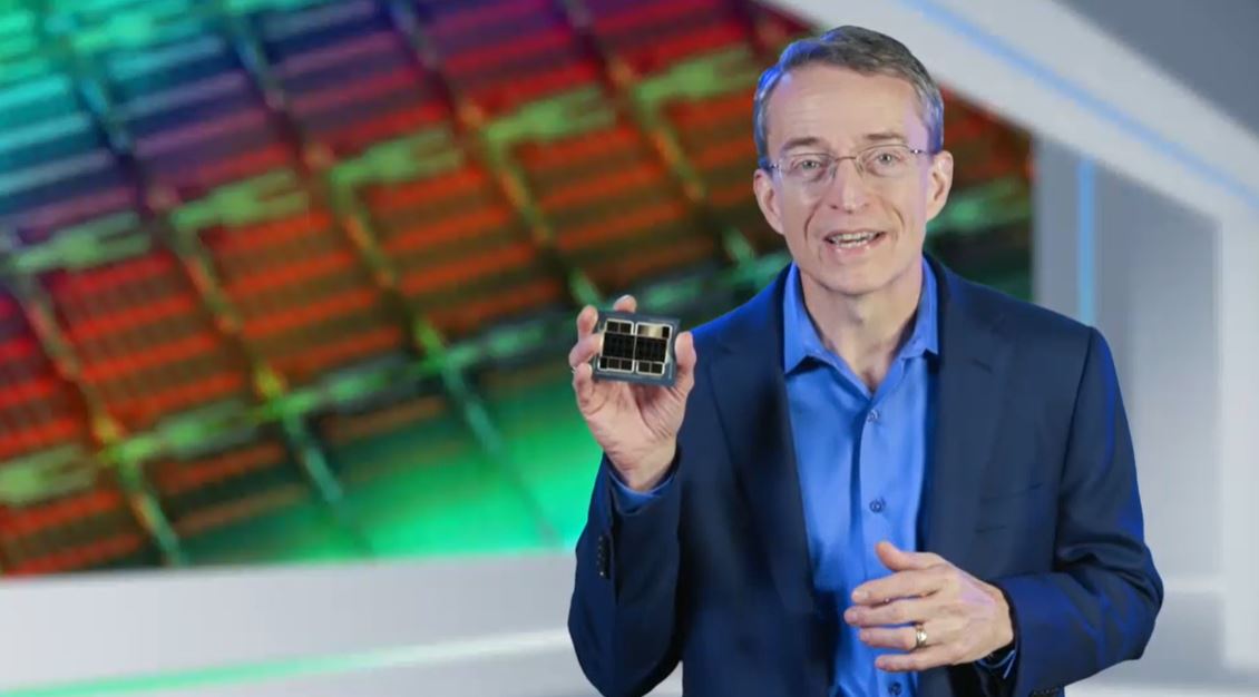
Ponte Vecchio utilizes ~40 tiles and uses Foveros/ EMIB technology. We are going to hear more about this in the near future. Still, this is several levels beyond chips like the AMD EPYC 7003 “Milan” series and the NVIDIA A100.
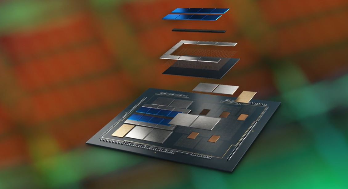
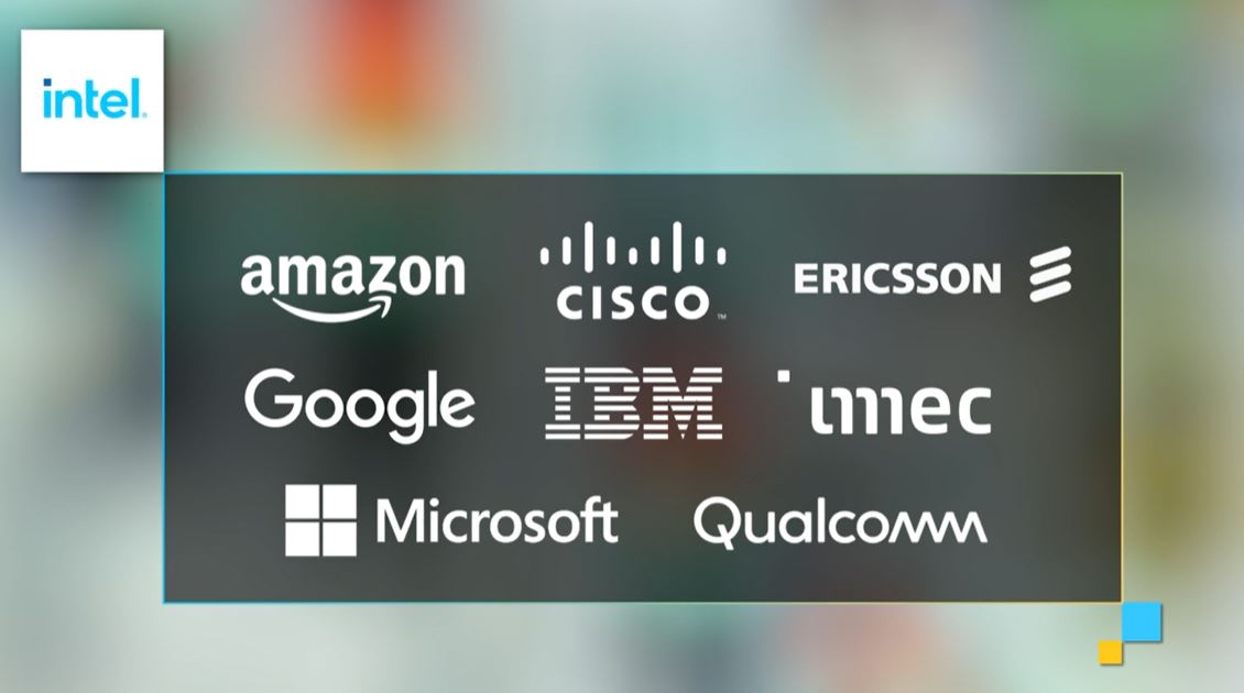
While that is a large and complex chip by today’s standards, it is also a showcase for things to come. Intel’s XPU strategy, and the future of chips is in creating packages of tailored IP. In the server space, this means a hyperscale client or government client may want more of some IP, less of another, and integration of custom IP. Intel’s packaging (and announcement today of a partnership with IBM for research collaboration on future generations) is a good example of how the company is looking at the future of chips.
The bottom line is that the Ice Lake Xeon that launches in about two weeks will effectively be the end of the monolithic die era in mainstream servers. To scale up in sockets IP needs to be broken up and technologies like Foveros allow multi-tile integration from different foundries/ processes to manage risk and get to bigger chips. AMD has had to do this for years, albeit nowhere near as advanced as Intel’s Ponte Vecchio/ Foveros.
Intel discussed Tiger Lake which is shipping now and the upcoming PCIe Gen5/ DDR5 Alder Lake slated for later this year. We covered the 11th Gen Intel Core Desktop Processor Rocket Lake-S Launch is happening on March 30, 2021, however, the enormous upgrade successor is expected only a few months later in the second half of the year.
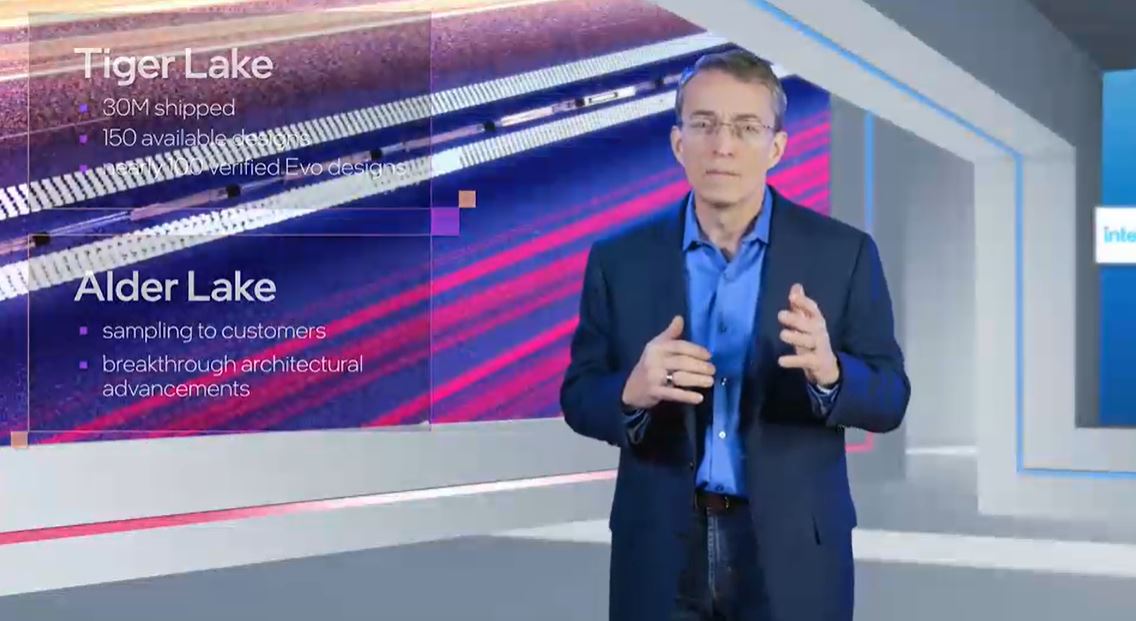
In terms of Ice Lake, that is coming on April 6, 2021. Still, the focus is on Sapphire Rapids which Intel says is coming with a volume ramp in 2022.

In the data center, Intel has been very clear that Sapphire Rapids is the big upgrade to its current line, well beyond Ice Lake’s new features.
That brings us to manufacturing and Intel IDM 2.0.
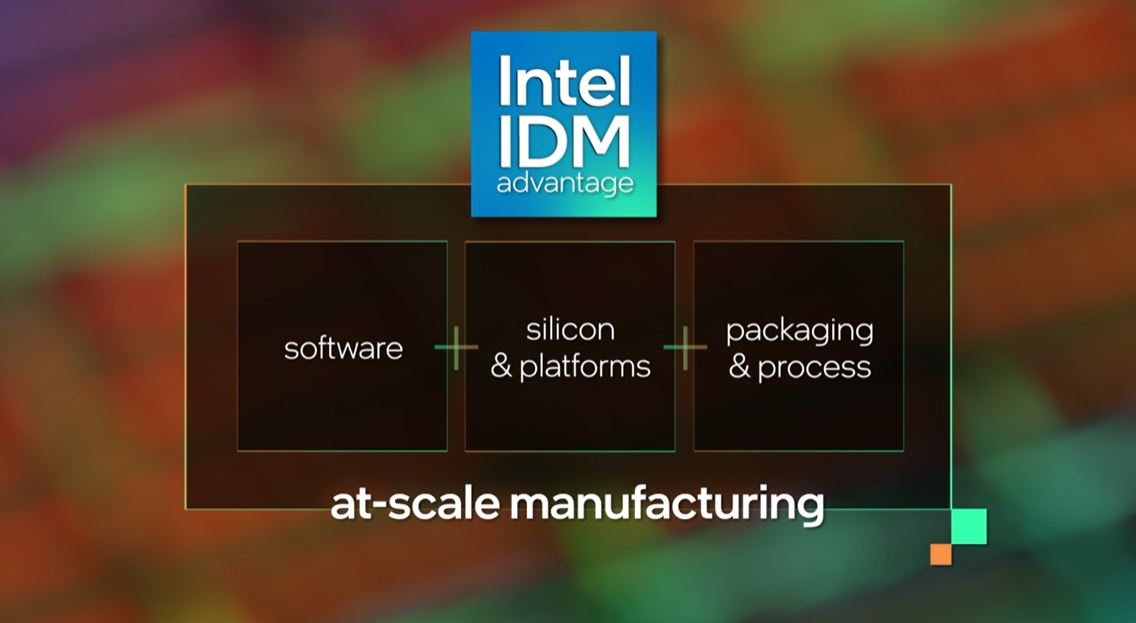
Intel IDM 2.0
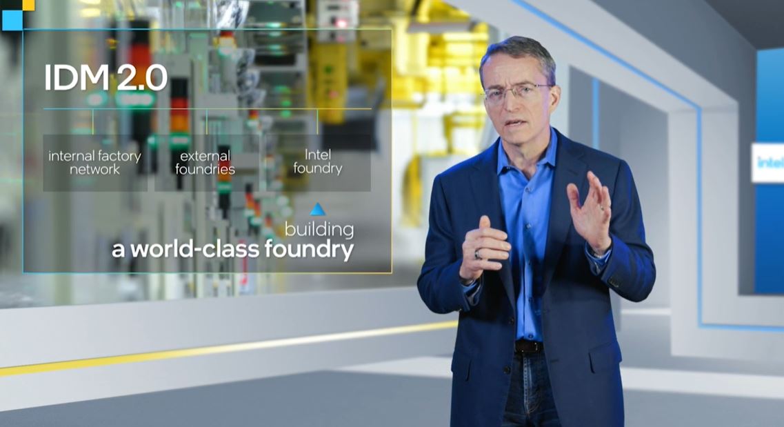
Intel knows it needs a revamp on its manufacturing image, and it is doing so today. The three pillars are Intel’s internal fab capacity, using external foundry partners, and starting a true Intel foundry business. Intel’s own factory network has struggled with new processes, but it also ships a lot of IP built on other foundry processes. Today, Intel noted that it will expand its purchases from TSMC, Samsung, GlobalFoundries, and UMC.
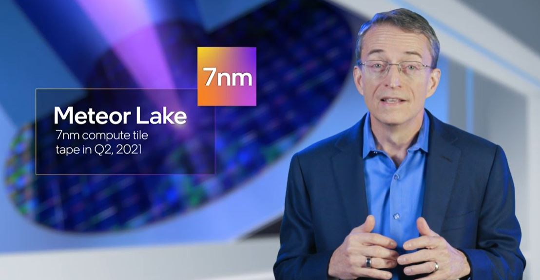
Intel was saying that its Meteor Lake “7nm compute tile” is being taped out in Q2 2021. This is important. Intel is already messaging that its x86 cores are going to tile even in the consumer segment. Instead of taping out a monolithic die, Intel is focused on a smaller 7nm compute tile. This was an example of 7nm process (which is to say getting beyond the challenge that is 10nm) win, but it is clearly messaging that Intel will be using IP blocks in tiles going forward across its range.
The big announcement though is that Intel wants to get into the foundry business. Really this time. Intel has dabbled in trying to do foundry, but it is creating a dedicated business unit with its own P/L, direct reporting to the CEO, and its own fab capacity.
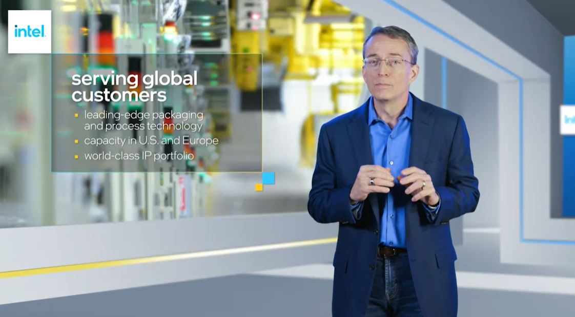
Intel said that it planned to open up more of its IP portfolio, making special note of opening its x86 cores, and also Arm and RISC-V for integration using other IP and its packaging.
The reason for this is fairly clear. First, foundries tend to have longer tails on their manufacturing lines. We saw, as an example, last week’s Xilinx Brings the COPs with Zynq and Artix UltraScale+ chips launching at a time when Xilinx’s top-end SKUs are using TSMC 7nm. The longer lines run, the better utilized installed equipment is. So 14nm++++ (how many are we at?) may become a popular foundry node at some point.
To this end, Intel is spending $20B for two fabs in Arizona. It also says that it plans to have more fab capacity being added in the US, Europe (we read this as Ireland), and elsewhere (Israel may be a candidate here) with announcements later this year. Intel sees the supply constraints on the foundry business and is trying to address them.

Intel briefly discussed that the US and EU (leaving the UK out of the discussion) are both looking for more local semiconductor manufacturing. Intel also said that its decision to build the $20B Arizona facilities was not related to the CHIPS legislation that would provide support for US domestic semiconductor manufacturing.
The new business unit is being called Intel Foundry Services. We shall see if this new model has a better outcome than the previous generation.
Intel IDF is coming back in a new form with Intel On in October 2021 in San Francisco.
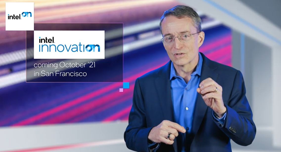
IDF holds a special place in Pat Gelsinger’s history at Intel, so the new Intel Borg captain is not going to let that piece escape assimilation.
Final Words
There was certainly a lot to unpack today. Pat Gelsinger has a clear goal: to go after an even larger TAM. Whether you purchase an Intel chip or one from its competitors, Intel wants to make that chip, or leverage a foundry relationship to get it made or package it together. The Intel Borg is only going in one direction, assimilating heterogeneous IP blocks no matter their origin into a number that can be part of Intel’s TAM.
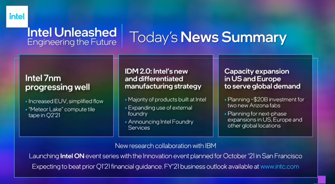
Overall, the announcement today makes a lot of sense. Intel’s alumni CEO hire wants to make his mark on the company. Setting up a multi-year big program to do so while hopefully expanding TAM is a good model. He also gave some honest feedback on the state of 10nm while giving a glimpse of Intel’s 7nm EUV tile and Foveros/ EMIB packaged future.
Part of why Intel’s board hired Pat was simply because it is the type of hire that can help energize employees and customers. While Pat was gone, most in the tech industry saw him as the leader of VMware so he added software credentials, a big deal looking to the OneAPI push and beyond. Intel’s board hired Pat for this type of enthusiastic push trying to change the direction of the giant ship that is Intel. Now we wait to see the outcome as things in the semiconductor space take years.



Well – If they are going to compete in the ARM SoC market, they probably need to speed up development of their processes then. They are quite far away from being able to get even close to the current state of ARM chips 7nm is just not going to cut it when they will be ready. (and it will probably not help them that much bashing Apple in their ads. Those Sour Apple’s might just come back to bite them in the behind.)
Now looking at it strictly as a business it does make sense what he wants them to do, but i’m just not sure they will be able to execute in time. They may be able to go into new markets in the AI and datacenter, but my guess is that there might just be enough old school internal war going on with leaders below Pat, that don’t want to give up what they have been doing for the past 20 years, that any kind of turns of their supertanker, will just be stalled long enough to delay any real response to the outside threats.
Intel needs to talk less and do more.
For those who didn’t know; TAM = Total Addressable Market. I can grok IT, but not marketing. =D
Pat should ask Patrick what Patrick recommends for Intel’s Optane inventions.
If Pat were to ask me, my initial answers are: ditch the VROC dongle,
open up the PCI-Express bus to encourage customer experimentation
with “4×4” add-in cards that span multiple x16 slots. The numbers
strongly suggest that PCIe Gen4 will easily surpass the max bandwidth
available from Optane DIMMs running at DDR4-2666. DOWN-CLOCKING
the entire DRAM apparatus, as Patrick has observed, is a terrible penalty
to impose on a server, and that penalty is something which Intel engineers
should have foreseen long ago! If Intel runs into patent restrictions,
Intel already knows how to cross-license with existing winners.
Lastly, I’m betting that a 10% reduction in Optane prices will increase
demand by 20% or more (read economic “elasticity”).
My 2 cents.
p.s. Just consider what happened with storage in general
when the reality of “upstream bandwidth” dawned on the IT industry
e.g. now it’s easy to install a cheap USB adapter and easily increase the
upstream bandwidth of standard USB 3.0 ports to 2.5GbE and 5GbE.
PCIe Gen1 x1 clocked at 2.5GHz, but the Gigabit NICs in millions of PCs
still clock at 1G!
Thus, we learned a lot by “syncing” storage with chipsets.
Now, we should see if the same is true if we “sync” storage with DRAM.