At this point, the OCP NIC 3.0 form factor has taken the world by storm, perhaps becoming OCP’s most impactful project to date. Our readers sometimes notice that while we generally say “OCP NIC 3.0” compatible servers and devices, there is a lot more going on in the actual several hundred-page spec. Instead of referencing the giant spec, we thought we would pull out the most important physical features to know for those that purchase servers. If you make NICs/ accelerators or are the electrical engineer doing work on the servers, the current spec is going to be more useful. For the broader market, here is what you need to know so we made a “bookmarkable” reference guide.
OCP NIC 3.0 Physical Form Factors: The Quick Guide
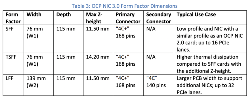
There are two fundamental widths an OCP NIC 3.0 comes in. W1 is perhaps the most common as it uses the 4C+ connector and is the common width we see for many NICs today. The W2 is one we see less commonly, but it is very interesting since it provides more PCB space as well as more PCIe lanes. This has the same 4C+ connector (+ for the OCP Bay connector) as W1 but adds a second 4C connector (without the +). The impact of this is that one gets 32x PCIe lanes since each 4C is 16 lanes.
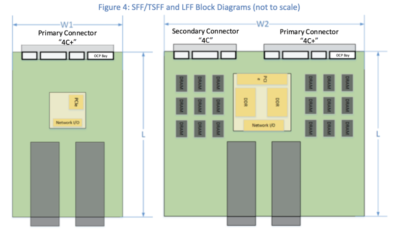
While the depth of OCP cards (currently) is 115mm, the height can be either 11.50mm or 14.20mm. SFF is 76mm x 115mm x 11.50mm. TSFF is 76mm x 115mm x 14.20mm. LFF is 139mm x 115mm x 11.50mm. We are going to note that there is a project looking at taller cards for higher TDP devices.
With those three basic form factors, let us get to the connectors since that is often something that is different.
OCP NIC 3.0 Connector
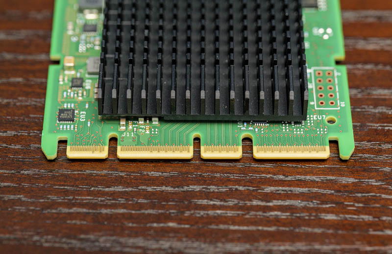
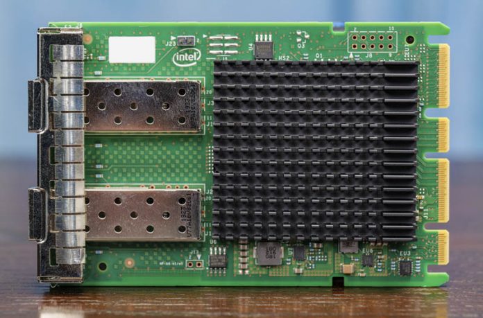
The standard OCP NIC 3.0 4C+ connector can be seen on this Intel X710-DA2 OCP NIC 3.0 card. The connector has two small blocks with a larger block in the middle for the x16 data lanes. The larger 28-pin block at the edge is the OCP Bay portion noted above that is designed to carry things like sideband signals.
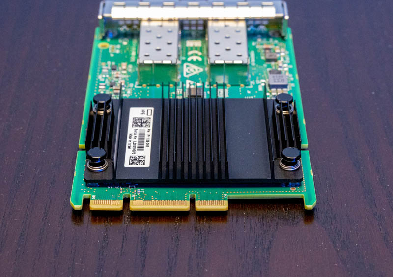
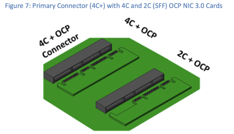
Sometimes, we see interesting implementations such as this HPE 25GbE NVIDIA ConnectX-4 OCP NIC 3.0 adapter that is missing the larger block. This is the 2C+ connector.
Here is the figure from the spec sheet that corresponds to the two connectors seen above. Per the spec, one can use fewer pins for less PCIe connectivity.
We have not had any/ many LFF cards in the lab, but you can see the LFF connector here where the top right has the 4C+ connector and the bottom left has the 4C connector. The primary connector always has the OCP Bay “+”.
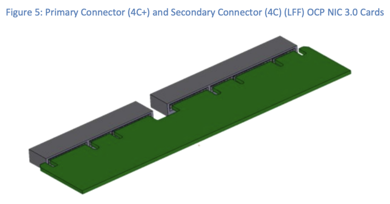
There is the option with LFF to not have the secondary 4C connector and just use the larger form factor with the 4C+ only for 16 lanes, providing more board area for components and cooling.
Most of our readers are going to encounter SFF or perhaps TSFF more often than LFF on servers. One of the big innovations with the OCP NIC 3.0 form factor is modularity. This is something we are also seeing with the EDSFF SSDs.
OCP NIC 3.0 Retention
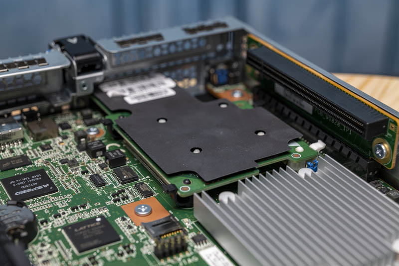
This is a huge one. Just to understand why here is an older Inspur server’s OCP NIC 2.0 form factor card installed. As you can see, servicing this card requires pulling out the node/ opening the chassis, and getting to the NIC.
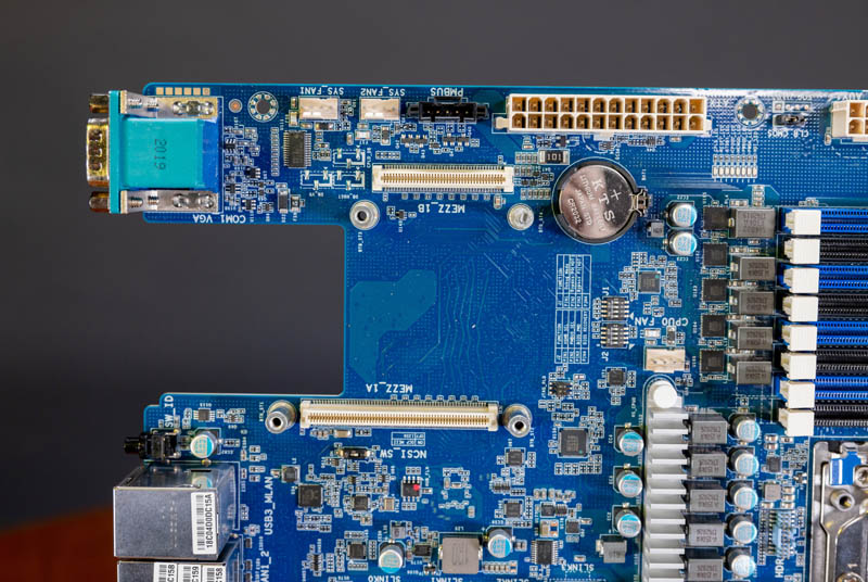
Here is the OCP NIC 2.0 mezzanine with both the A and B connectors for reference. The innovation in that generation was the standardization of the mezzanine. Before the OCP companies decided to standardize, Dell, HPE, Lenovo, and others all decided to make proprietary NIC mezzanine modules. That lowered the volume of the modules and therefore the quality (because lower volumes mean less deployment and testing against the specific module.) OCP NIC 2.0 was the hyper-scalers approach to making a more reusable ecosystem.
Contrasting the above Inspur OCP NIC 2.0 installation to the company’s OCP NIC 3.0 installation, one can see that the newer 3.0 module is designed to be rear serviceable, with an asterisk. Inspur’s design here is rear serviceable so one can remove the NIC without having to disassemble the chassis as we do for our server reviews.
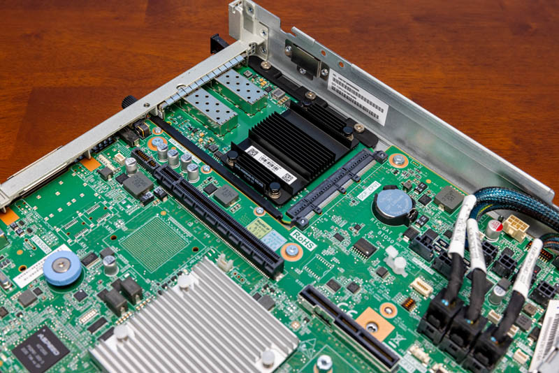
Companies like Dell EMC that rely on hefty service contracts for higher margins are able to use a different latching mechanism in order to make the OCP NIC 3.0 more difficult to service. This retention mechanism requires opening the chassis to disengage this latch before changing the NIC.
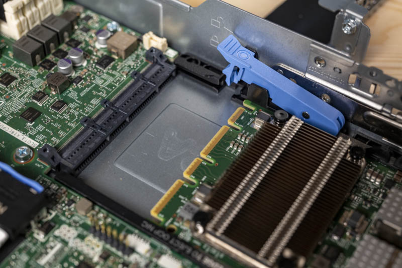
The reason we see these two different models, aside from the business reasons, is because there are actually different retention mechanisms. Since the cards are designed to be rear serviceable by hyper-scalers, the spec needs to ensure that pulling a SFP or RJ45 connection does not take the entire card with it. That leads to three different latching mechanisms:
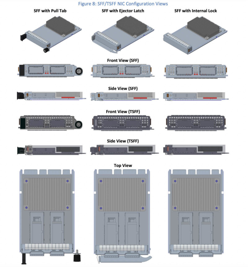
Perhaps the most common designs we see are the SFF with Pull Tab design. This uses a screw on the side of the faceplate to keep the module in place. Servicing theses simply requires unscrewing the thumbscrew and then these can be serviced completely outside the chassis.
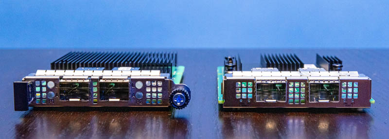
The SFF with Ejector Latch has an ejector latch arm that locks the NIC in place. The SFF with Internal Lock is the version shown above in the Dell C6525 example. That generally requires slightly less faceplate space, but trades serviceability for that small space gain. An internal lock is required because that is how the NIC is held in place preventing accidental removal when a network cable is removed.
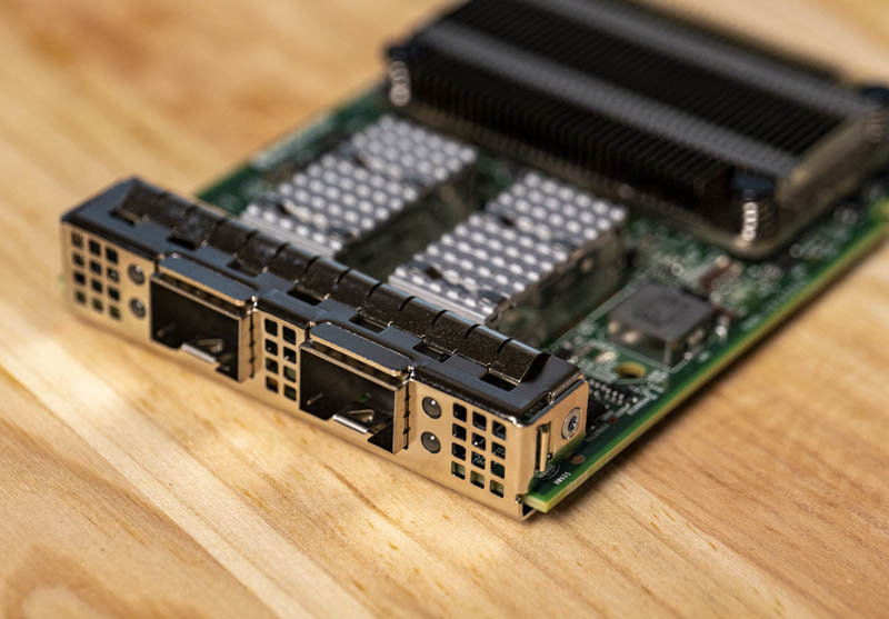
Something you will notice is that the spec is designed for the card manufacturers to build a card, and then have different retention mechanism hardware added to complete the module. One of the big challenges with OCP NIC 2.0 was always the faceplates.
The LFF modules use ejector latches that can be either short or long in length.
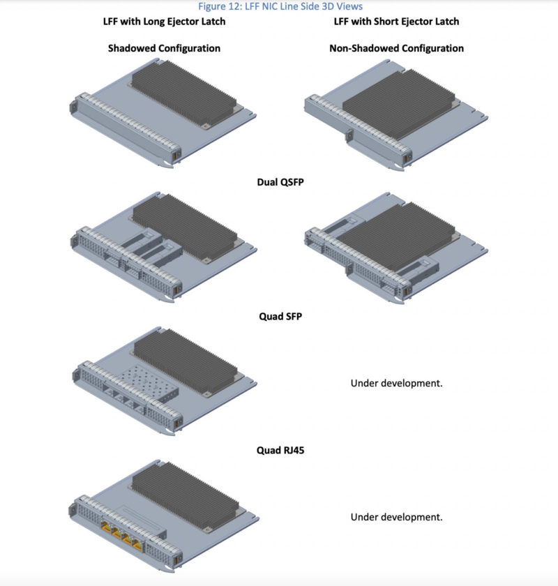
Hopefully we can get photos of some of the larger cards soon, but right now most of the modules we have seen are SFF.
Going Beyond NICs with OCP NIC 3.0
OCP NIC 3.0 is interesting for more than just NICs. There is little reason that a company cannot put PCIe retimers, switches, or other devices on an OCP NIC 3.0 card given that it can handle 16-32 PCIe lanes. At OCP Summit 2021, we saw Broadcom HBAs and Tri-Mode adapters that were built into the OCP NIC 3.0 form factor.
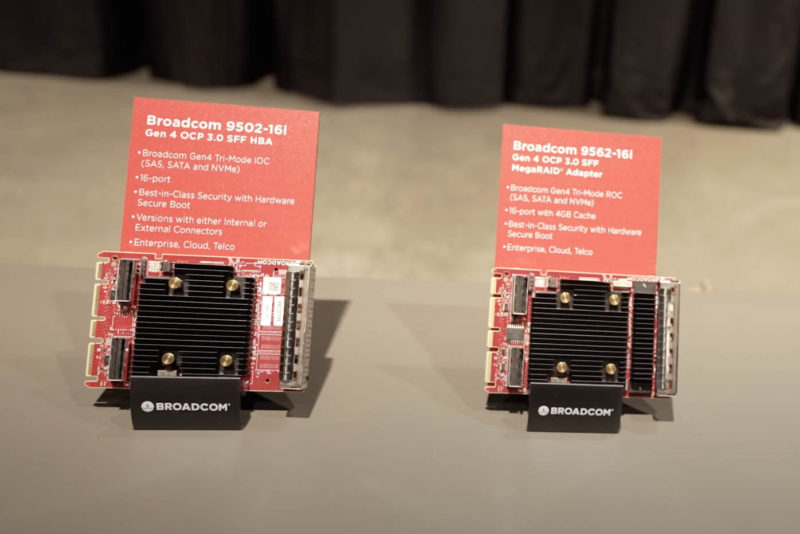
Power and cooling and space can be challenges, but for many applications this is a form factor we expect to see more of in the PCIe Gen5 era that we are going to enter later in 2022.
Final Words
Our goal with this piece was to make a practical guide to understanding the OCP NIC 3.0 form factor. It is surely far from perfect, and there is a lot more documentation out there. We just tried to pull the most relevant information for those who are not designing products but instead using OCP NIC 3.0 cards in their servers.
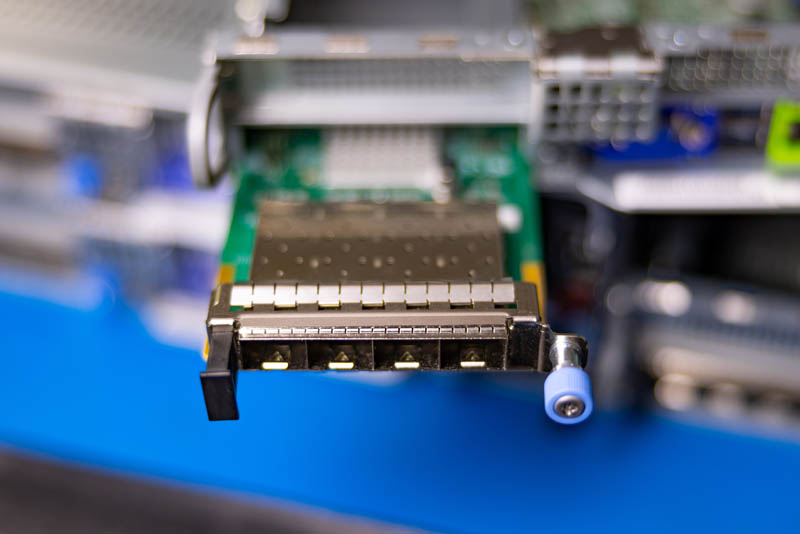
Hopefully this can be a quick reference guide to help you understand what is being used in a given server.



I have seen a PCIe to OCP 3.0 adapter card from Teledyne Lecroy, but it loads the OCP card vertically.
Has anyone seen an adapter that allows an OCP 3.0 card to be installed into a PCIe slot horizontally, where the I/O connectors would be on the same externally facing plane as it would be on a normal PCIe NIC?
I have an X710-DA2 PCIe card and OCP 3.0 card in my lab. Comparing them, it sure seems like it would be possible to have a PCIe adapter that you could feed an OCP 3.0 card into.
Not sure if there is a real practical application beyond testing, but sure seems like it would be possible. thoughts?
I didn’t get the point about the latching mechanism, why would you not want to be able to service the module without having to open up the server?
Supermicro’s AIOM is not compatible with this OCP connectors, right?
AIOM is SFF OCP3 with pull tab. On Supermicro’s marketing they say it is.