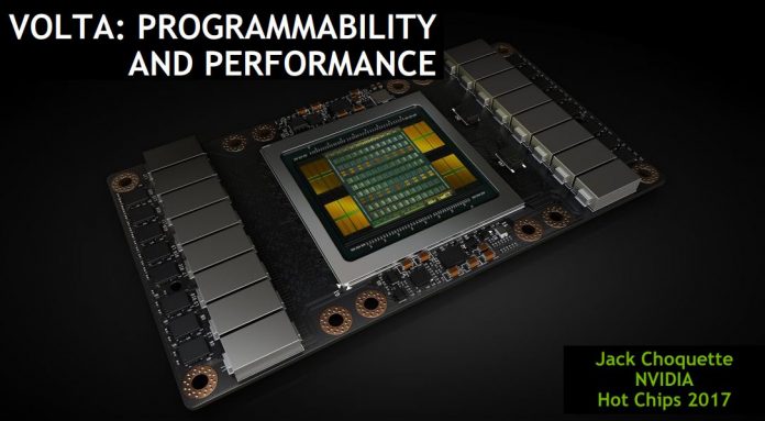
At Hot Chips 2017, NVIDIA presented more information about their new Volta architecture. Specifically, the topic was the NVIDIA Tesla V100 GPU. We previously covered the NVIDIA Tesla V100 at GTC 2017. In the meantime, NVIDIA has started to ship the Volta based GPUs in limited quantities and this quarter we expect the DGX-1 to get its V100 update. In the deep learning space, this is the generation where NVIDIA hardware is clearly leap frogging AMD’s newest offering.
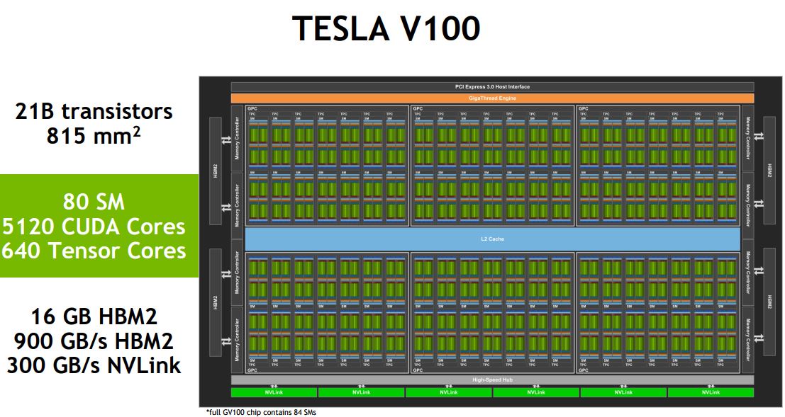
One can see here that the NVIDIA Tesla V100 has 80 SMs active. The small footnote on the slide we could see clearly from our seat. It says that a full GP100 chip contains 84 SMs so NVIDIA is binning products to enable higher yields.
In terms of performance, the NVIDIA Tesla V100 numbers are sometimes staggering for a generational improvement.
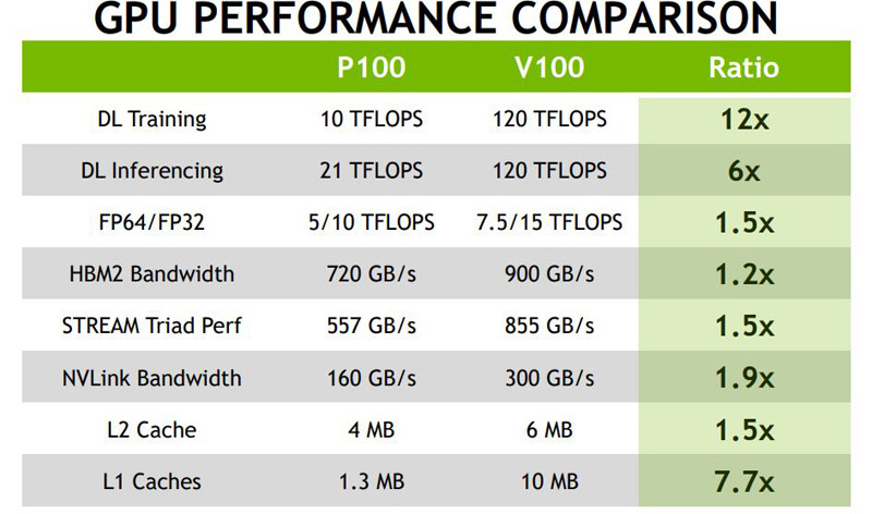
The key here is that NVIDIA is moving to larger caches, and adding specific accelerators for the deep learning space while beefing up overall bandwidth.
We did want to take a second and show the depiction of the SM core. One will notice that the SM core has large Tensor Cores. It is clear what NVIDIA’s focus is for this generation.
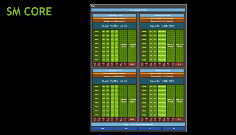
From the illustration, this is a ton of die space dedicated to Tensor Cores. One has to wonder whether NVIDIA will make the decision to bifurcate its deep learning chips from its consumer/ video chips with this generation. It becomes hard to fathom how costly this would be on a gaming GPU where it would get little to no use.
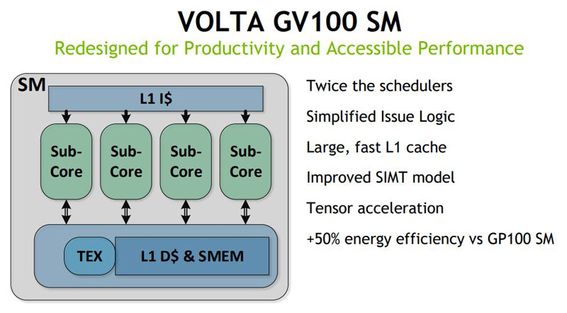
We are not going to spend much time regurgitating the text NVIDIA presented on the SM side. Like most architectural advancements, the new NVIDIA Volta GV100 SM is designed for more performance.
Likewise, here is the microarchitecture view:
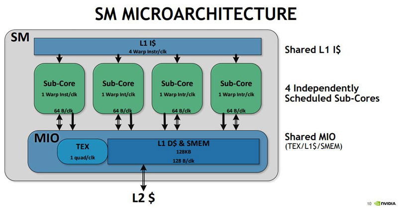
And the sub-core view:
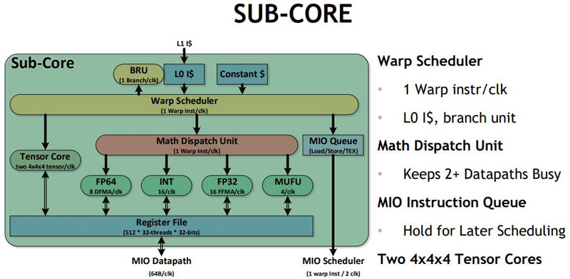
Key here are the two 4x4x4 Tensor Cores. That is the secret sauce that is making Volta a revolutionary leap over an evolutionary one.
One other area NVIDIA spent time on was the L1 cache and shared memory.
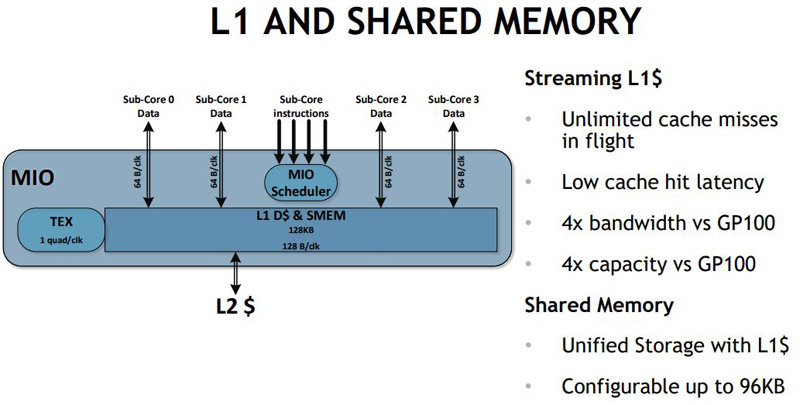
One can now dedicate cache as shared memory if you know your workload can take advantage of such data locality. As NVIDIA beefs up L1 and L2 caches, we are seeing a much more compute driven architecture than something required for gaming.
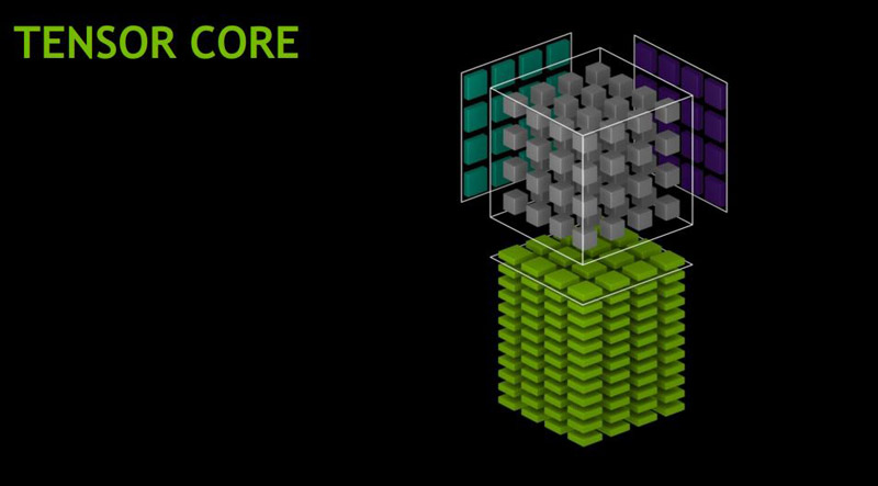
The Tensor Core is the allows one to do mixed precision matrix math using 4×4 matrices.
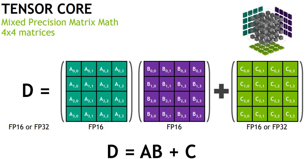
This is a key operation when training deep learning models. With improved scheduling, NVIDIA can do 16×16 matrix math.
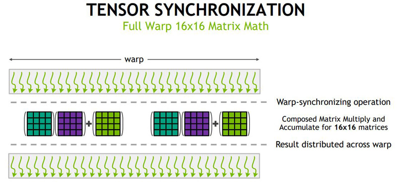
Here is another view NVIDIA presented on the Volta tensor operation showing how one can use lower precision FP16 inputs and arrive at a FP32 output.

In terms of impact, NVIDIA claims that some operations will see a 9.3x speedup.
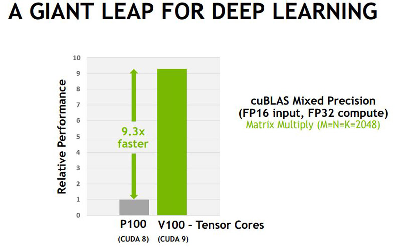
We do want to note here that NVIDIA is combining CUDA 8 to CUDA 9 software gains along with hardware gains in a specific workload.
NVLINK Updates
NVIDIA is claiming that the new GV100 NVLINK will offer even more bandwidth of up to 1.9x what we saw with the GP100.
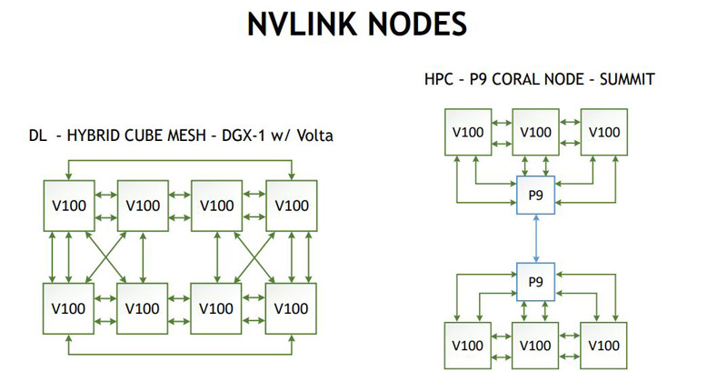
The GV100 will have up to 6 NVLINK connections which allow for a number of topologies to facilitate GPU to GPU connections. This is certainly a much higher-end way to get more GPU to GPU bandwidth than we have seen in servers featuring PCIe switches. Single Root v Dual Root for Deep Learning GPU to GPU Systems.
Final Words
There are a few key takeaways from the NVIDIA Tesla Volta V100 presentation. First, it is clear that driving data center sales is an architectural goal of this generation of products. Second, one does have to ponder whether all of this added logic makes sense in consumer parts. One of the keys to NVIDIA’s success in the deep learning space has been that high-performance CUDA training could happen on the desktop using the company’s gaming GPUs. From the diagrams, NVIDIA is showing, and the logic portions, one has to wonder whether the Tensor Core will be part of the gaming line in any form. While we would expect the NVIDIA Tesla V100 to have premium features at the price, there appears to be a lot of silicon in the V100 design dedicated to non-traditional GPU (gaming) tasks.

