NVIDIA H100 or L40S in Supermicro SYS-521GE-TNRT Servers
Something very different with today’s systems is that they are now a full 5U. This is generally because the TDP of each GPU, H100 or L40S is 350W. Commonly, these systems have eight GPUs for around 2.8kW in the GPUs. The other reason is that between the two options, these systems are typically using power in the 4.3-5kW range. That makes them enough for a single server per 208V 30A rack or several servers in a higher-power rack. Density is less challenging with modern AI servers since often power and cooling in racks is the bigger limiter.
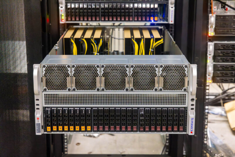
That extra 1U of space allows for more cooling to the GPUs. NVIDIA GPUs and the H100 and L40S follow this lead and typically can use their maximum rated power, but they also usually use less than their rated power on average.
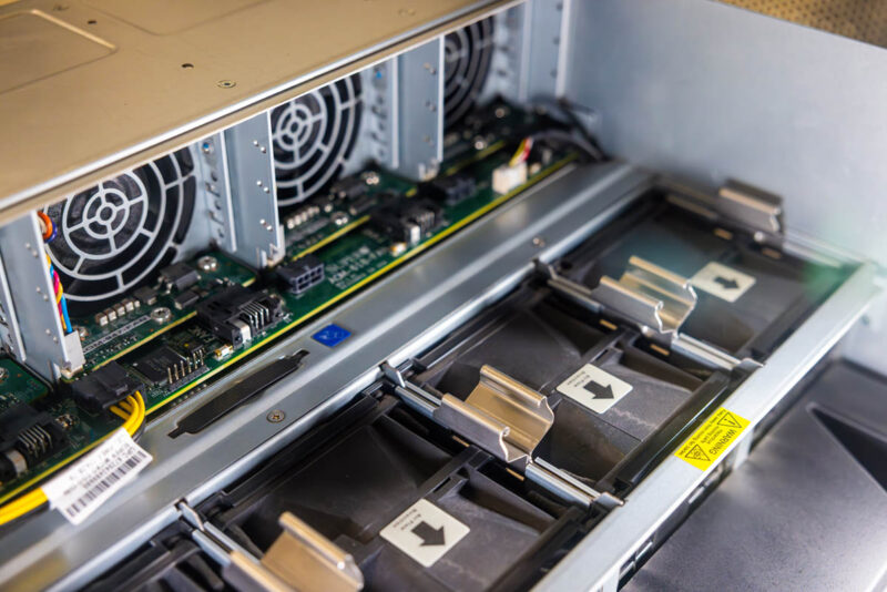
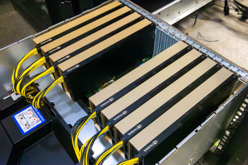
Supermicro has both Intel Xeon and AMD EPYC versions of the chassis. We had two Intel Xeon versions set up, one with 8x NVIDIA H100 GPUs.
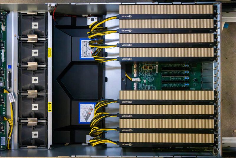
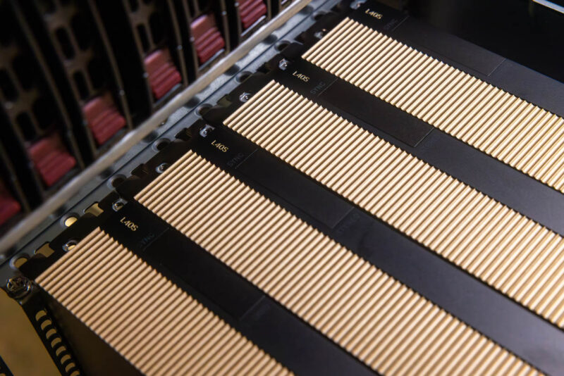
And the other with the NVIDIA L40S cards.
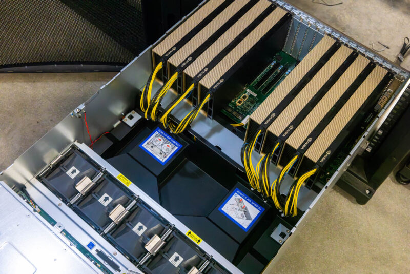
You can see that these are set up with only eight cards, but these systems can scale up to 10, as we used in DeepLearning11 way back in the day.
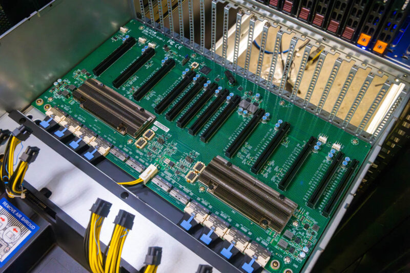
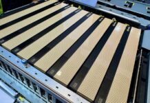
With PCIe GPU servers, how GPUs are connected is important for things like P2P across a PCIe switch without NVLink, and how well NVIDIA NCCL works on the workload. NCCL is important to scale out jobs to multiple GPUs. The Supermicro SYS-521GE-TNRT uses PCIe Gen5 switches in a dual root configuration. One can see the two PCIe switches under heatsinks on the GPU board, and that board is cabled between the switches and the CPUs in the systems.
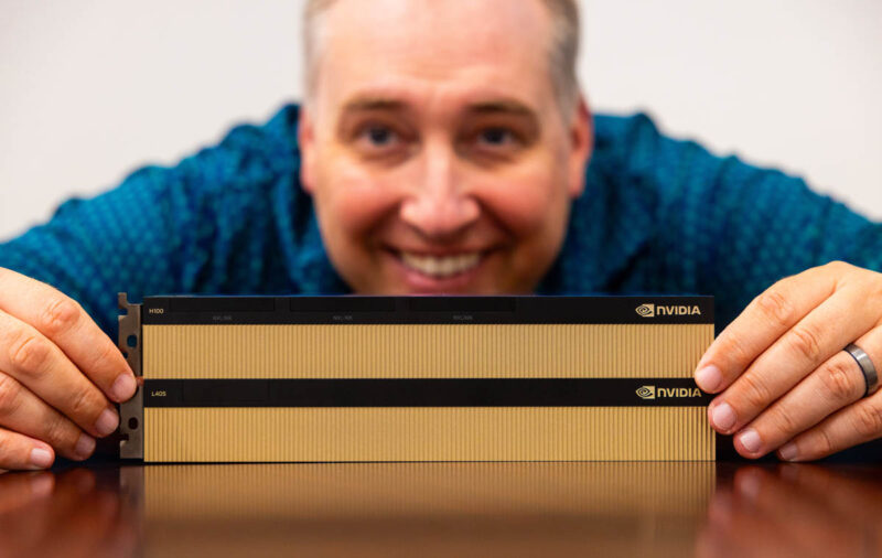
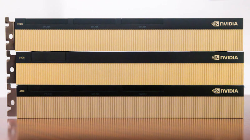
The NVIDIA H100’s can be installed in this server using the NVLink bridge connecting cards in pairs. Looking at the L40S, everything is PCIe.
Performance Summary
We ran LLaMA 7B inference on these GPUs. We only had a very short amount of time where we had access to them, so that limited what we ran. NVIDIA publishes a lot of numbers for AI, so feel free to browse those. We will hopefully get to update this piece with a few more over time.
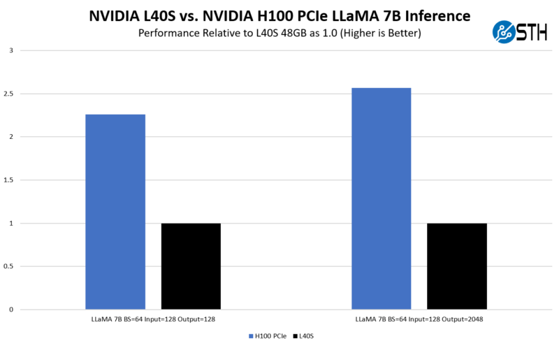
We checked our results versus NVIDIA’s official numbers. On the official results, NVIDIA is using its H100 SXM5, not the PCIe version, but we use a rule of thumb that the SXM5 version is around 25% faster (but it varies based on workload) than the PCIe version and it feels like we are in the ballpark.
That brings us to the obvious: why the L40S if the H100 is faster? It turns out that folks are deploying these because 48GB is enough memory, especially using FP8, to be more than competitive with the A100, even the SXM version, using FP16. On the other hand, we generally see a H100 PCIe is 2.0-2.7x the speed of the L40S, but it is also 2.6x the price. The L40S is also available much sooner than the H100, and some deal pricing put the L40S at a level even more competitive with the H100, tipping the scales even more in favor of the L40S.
There are a few caveats. If you are deploying over 10,000 GPUs, NVIDIA is focusing on not just the H100 but also the H100 SXM5 in the Delta Next platforms with NVSwitch and other technologies. We asked NVIDIA about this, and if you are “only” deploying 4000 GPUs (likely ~$50M+ of hardware), for example, the L40S is the go-to solution.
Other Considerations of the NVIDIA L40S vs. H100
There are several other aspects to consider on the L40S. One is that it supports NVIDIA Virtual GPU vGPU 16.1, whereas the H100 is still only supported with vGPU 15. NVIDIA is splitting its AI chips a bit from the vGPU support side.
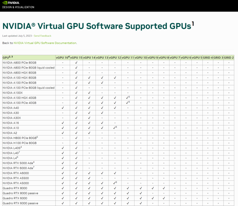
For those who want to deploy one kind of GPU machine and then be able to run different types of workloads, then something like the L40S makes sense. It also has the NVIDIA video encoding engines with AV1 support and RT cores, given its visualization roots.

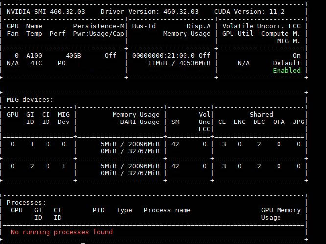
There is one feature the L40S does not support, and that is MIG. We have looked at MIG previously, but it allows a H100 to be split into up to 7 partitions of different sizes. This is mostly useful to split the H100 GPU in public clouds so that the GPU resources can be shared across customers. For an enterprise, this is usually a lower-excitement feature.
Also, deploying the L40S is a lower power affair, half the power of the SXM5 systems. That makes it very attractive for those who want to scale out but may not have huge power budgets for each rack.
The bottom line is that the L40S is not as fast as the H100, but it with its FP8 and Transformer Engine support from NVIDIA, it is an option that is more available and easier to deploy for many than the H100, and often at a lower cost.
Final Words
There is a lot of really poor information out there on the NVIDIA H100 PCIe versus the L40S and why one would use either version. Hopefully, this helps clear that up to a larger extent. To us, the L40S does not feel inexpensive, but it reminds us of 6+ years ago when the thing to do in AI was to use lower-cost NVIDIA GPUs in servers but then use more of them. NVIDIA has that model again, using the L40S and an officially sanctioned architecture that supports up to several thousand GPUs.
A quick thank you to Supermicro and NVIDIA for supporting this one. This seems to be a question we have been getting, along with simply what is a good H100 alternative architecture that is still NVIDIA. The L40S is really the answer for many customers.




The L40S is basically the datacenter version of the RTX 4090 with double the memory. Just shows you that Nvidia is so dominant in this segment that they can purposefully hamstring their consumer GPU to protect their datacenter cards.
That nVidia hamstrings the *102 cards for half precision is well known. They’ve been doing it since Ampere IIRC. Note how this L40S has no FP64 at all… can’t be offering anything that makes a general purpose GPGPU card for less than top dollar. nVidia has only offered this card because it can’t get enough chips for H100: if it was not supply constrained then nVidia would *never* offer this.
Perhaps AMD’s ROCm code getting knocked into shape even on Navi3 has some effect as well.
Which is better, 4x L4 cards or 2x L40S cards? Working on a budget here.