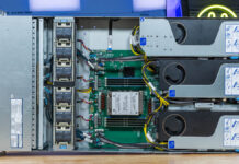
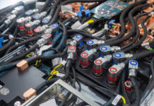
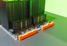
NVIDIA had one of the more interesting updates this week at SIGGRAPH 2023. The NVIDIA L40S is a 350W PCIe card GPU with more performance than the NVIDIA L40. In case you were wondering, since we only received a stock press image for this GPU, we decided to use Adobe Photoshop Beta for its generative fill for the images here.
NVIDIA L40S GPU for Data Center Visualization Launched
The new NVIDIA L40S has many of the same specs as the previous NVIDIA L40. The NVIDIA L40 is designed to be packed into PCIe servers where chassis airflow cools the GPUs. We have reviewed many of these over the years with cards like the NVIDIA A100, but cards like the NVIDIA A40 48GB GPU have been popular as well. The NVIDIA L40 and L40S are the successors to the A40 in many ways.
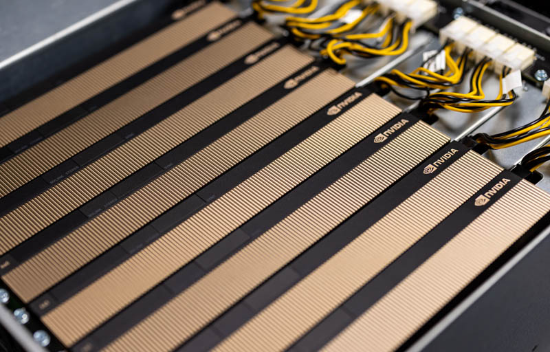
If you saw our cover image for the NVIDIA A40 review, you will see a good example of a deployment for the L40 and L40S.
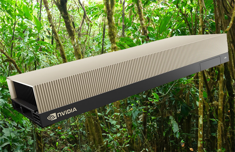
Here are the key specs of the new card:
| Architecture | NVIDIA Ada Lovelace Architecture |
| Foundry | TSMC |
| Process Size | 4nm NVIDIA Custom Process |
| Transistors | 76.3 billion |
| Die Size | 608.44 mm |
| CUDA Parallel Processing Cores | 18,176 |
| NVIDIA Tensor Cores (4th Gen) | 568 |
| NVIDIA RT Cores (3rd Gen) | 142 |
| Peak FP32 TFLOPS (non-Tensor) | 91.6 |
| Peak FP16 Tensor TFLOPS with FP16 Accumulate | 366.5 | 733* |
| Peak FP8 Tensor TFLOPs with FP16 Accumulate | 733 | 1466* |
| Peak TF32 Tensor TFLOPS | 183 | 366* |
| Peak BF16 Tensor TFLOPS with FP32 Accumulate | 366.5 | 733* |
| Peak INT8 Tensor TOPS | 733 | 1466* |
| Peak INT4 Tensor TOPS | 733 | 1466* |
| RT Core Performance TFLOPS | 212 |
| GPU Memory | 48 GB GDDR6 with ECC |
| Memory Interface | 384-bit |
| Memory Bandwidth | 864 GB/s |
| Interconnect | x16 PCIe Gen4 (no NVLink) |
| Max Power Consumption | 350W |
| Graphics Bus | PCI Express 4.0 x16 |
| Display Connectors | DP 1.4a Supports NVIDIA Mosaic and Quadro Sync |
| Display Max Resolution / Quantity | Up to four 5K Monitors @ 60Hz per card or dual 8K displays @ 60Hz Each display port can support 4K @ 120hz with 30-bit color |
| Form Factor | 4.4” H x 10.5” L – Dual Slot |
The biggest difference seems to be the 350W power, up from 300W on the L40. Adding more power increases the average clock speed the GPU can run at and therefore increases performance.
Final Words
The L40S is interesting because it was not long ago where a 300W GPU in a PCIe card slot was considered a practical limit. Using GDDR6 instead of HBM lowers the cost of the cards and therefore can make these attractive cards for either remote visualization or even some forms of GPU compute.
Since these are designed to run applications like generative AI for creative professionals, it seemed to make sense to generate a few fills for the background of the card.

Do these cards support nvLink to combine multiple instances? My impression is that that A102 chip has nvLink support but nVidia hasn’t provided it in any A102 based cards thus far.
L40 doesn’t support NVLink, I doubt this one will either. I believe no Ada cards support NVLink, only Hopper.
No one likes Nvidia playing games with the mid-market datacenter lineup like this. We could use some genuine competition.
@ssnseawolf
Oh, it is disappointing! It is very useful when 2 card GPU memory is unified and seen as one continuous memory from the software to render more complex scene with more g-buffers.
The previous generation had easy 2-way nvLink support with nVidia only offering 4-way support in their DGX workstations. Limiting memory space to a single card doesn’t give users of the previous DGX generation a reason to upgrade. In some respects it’s ultimately be a step backward then.
WHOA. Something is going on with the Tensor cores. The L40S is about twice as fast as the L40 for all tensor operations other than INT4 (and INT1 is left unspecified for both).
Cliff – Suggestion, Add the L40 specs along side the L40S in that table in the middle.
Bold anything different/new on the S.
Will you have an L40S tear down available soon?