At STH, we expect that NVIDIA is going to release some crazy new data center gear at GTC 2022. It needs to with Intel entering the market with Ponte Vecchio and the AMD MI250X. Since the Ampere A100 generation launched in May of 2020, NVIDIA has massively expanded its portfolio with new networking gear, DPUs, and even the Arm-azing Grace Arm CPU-NVIDIA GPU combination. We are going to cover the announcements, here, then some of them we will cover in follow-up pieces later.
This is being done live so please excuse typos. Also, we have a NVIDIA GeForce RTX 3080 Ti GTC 2022 Giveaway that we are running alongside GTC this year. The entry form and details are below.
NVIDIA GTC 2022 Keynote Coverage Crazy New Data Center Gear
Let us get going with the keynote already! If you want to watch along:
We are probably going to fall behind at some point during the keynote but will catch up later so consider this a semi-live experience.
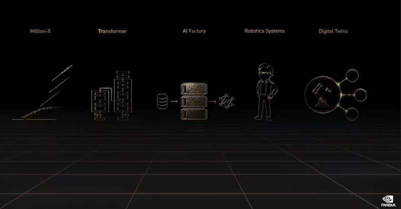
There were certainly data center views in the opening before Jensen got on. This is going to be an exciting day!
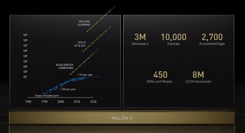
Jensen is saying that the CUDA and full-stack approach has led to a million-X speedup.
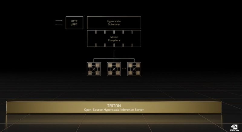
NVIDIA is discussing Triton. This is a large hyper-scale inference server. The company is supporting not just its GPUs but also things like AWS Inferntia accelerators and x86 CPUs.
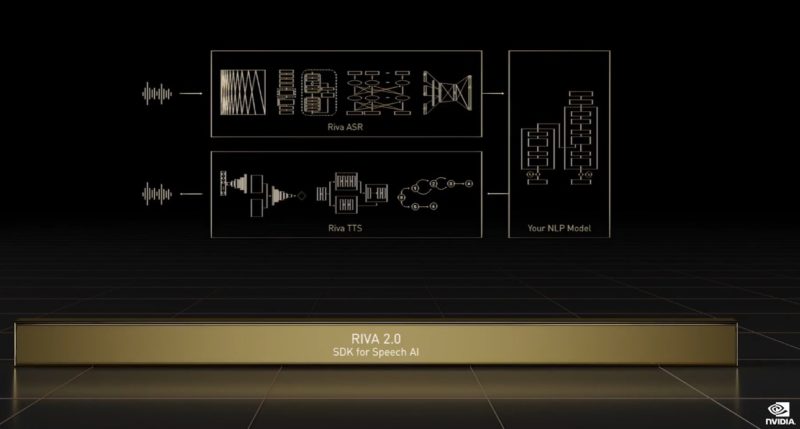
Riva 2.0 is for speech recognition and generation. NVIDIA is making this available so users can customize and return. We are not going to cover Maxine for video conferencing and some of the other frameworks but are going to pick a few.
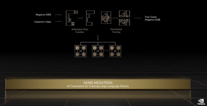
NVIDIA has its new recommendation engines and also things like Nemo Megatron for giant language models.
NVIDIA H100 Hopper Launched
This is perhaps the biggest one of today. More transistors, HBM3 memory on TSMC 4N, and huge 4.9TB/s of overall bandwidth. For this 4.9TB/s NVIDIA says 3TB/s is HBM3 bandwidth. There is a 0.9 TB/s Gen 4 NVLink. 0.9 TB/s of NVLink-C2C and 0.128TB/s of PCIe Gen5.
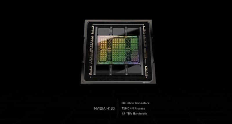
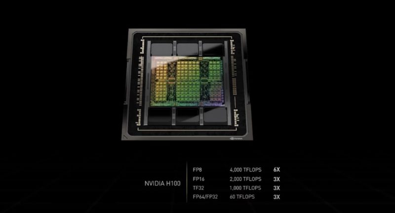
NVIDIA has a new FP8 format to increase performance along with new NVLink and PCIe Gen5.
The NVIDIA H100 is designed for up to 700W in SXM modules, it will be half of that in PCIe form factors also making it the hottest PCIe GPU at 350W.
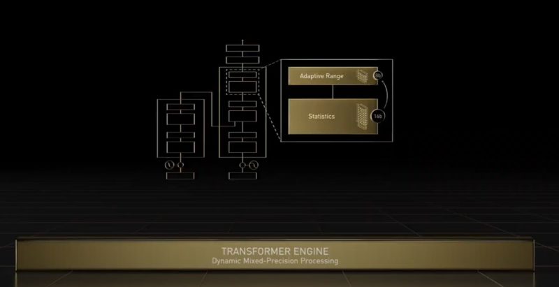
NVIDIA has a new transformer engine for FP8 and FP16 and acceleration transformer networks.
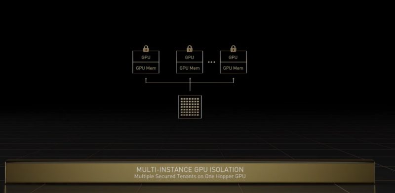
The H100 has a 7 MIG instance setup, like the A100, but it has the ability to have secure enclaves to allow multi-tenancy. Confidential computing is coming to GPUs.
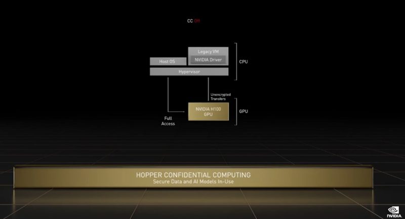
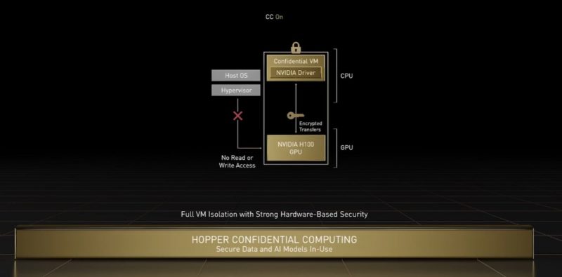
NVIDIA is also encrypting not just the in-flight data and application on the GPUs, but it will also be encrypting NVLinks and more in its 2022 generation of products.
NVIDIA also has its new DPX instructions to help accelerate some algorithms.
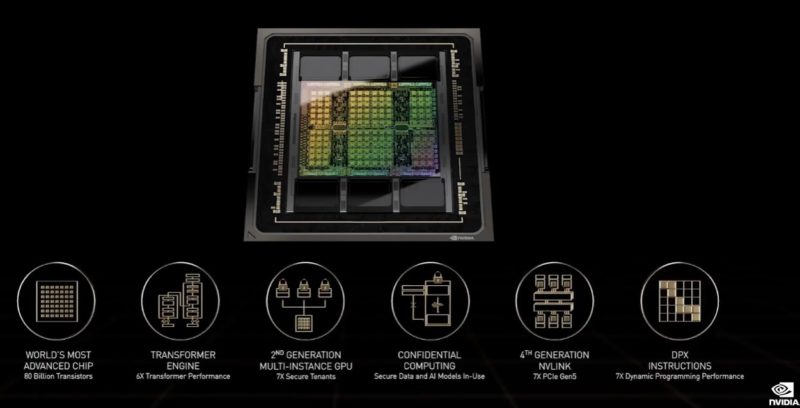
Here is the H100 SXM module. We asked about the six HBM3 packages, and NVIDIA said that there are six for the 80GB GPU for yield reasons.
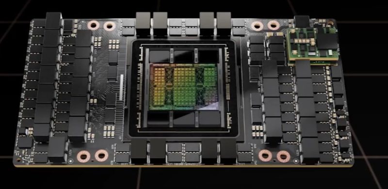
Here is what the HGX H100 will look like. As you can see we have the NVSwitch chips, but we also have liquid cooling. These are 700W GPUs. We also expect late Q2/ early Q3 that we are going to see early samples to OEMs, so expect to see Q3/Q4 the H100 start to generate a lot of buzz.
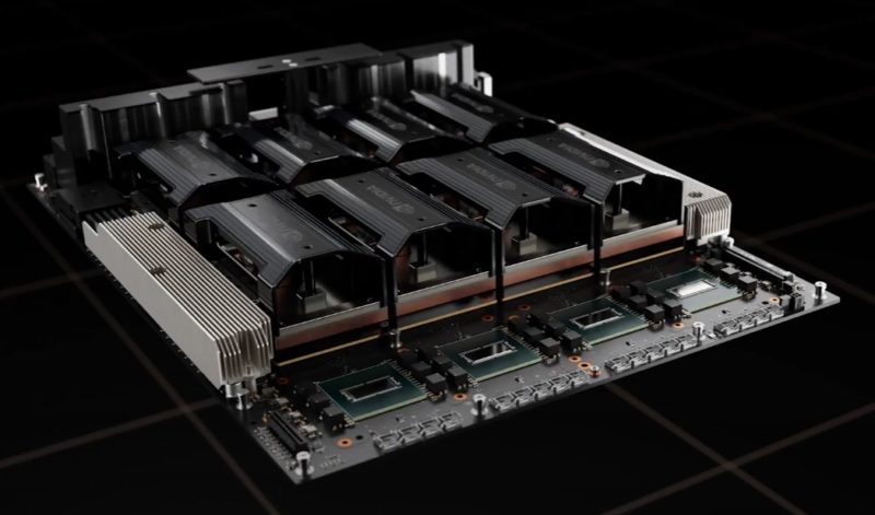
NVLink will have more security and encryption in this generation along with higher speeds and the ability to scale outside of the chassis using optical cabling.
NVIDIA said there are two PCIe Gen5 CPUs, even though none are currently on the market. That gives us some hint of when these will be available.
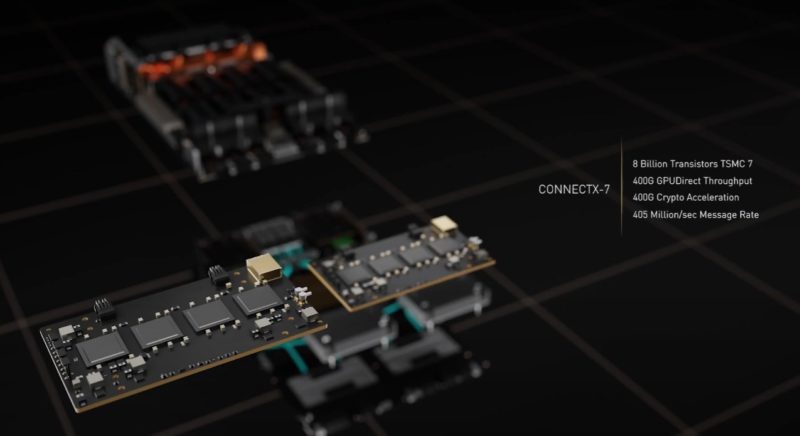
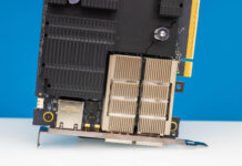
NVIDIA also has two ConnectX-7 modules.
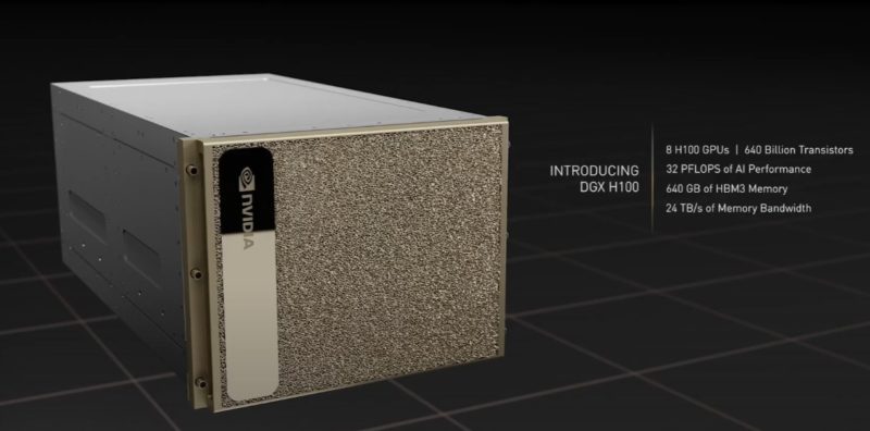
Here are the specs on the DGX H100 and the 8x 80GB GPUs for 640GB of HBM3.
Here is the look at the NVLink Switch for external connectivity.
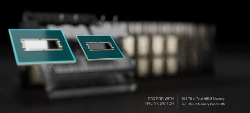
This allows DGX systems to scale to more GPUs.
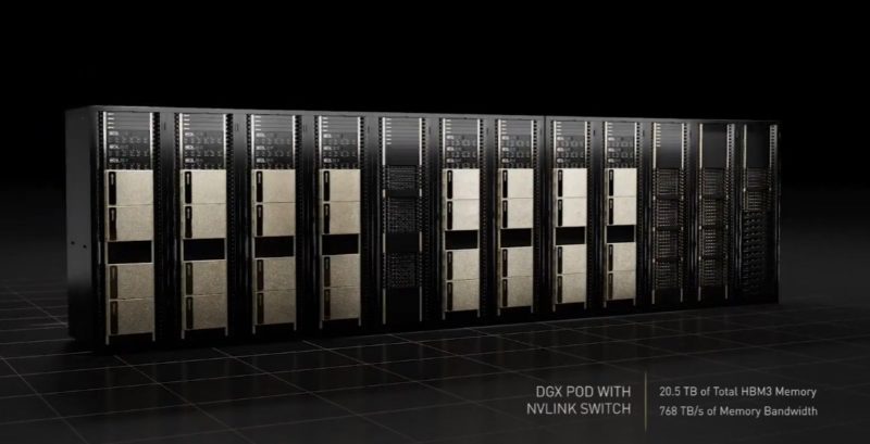
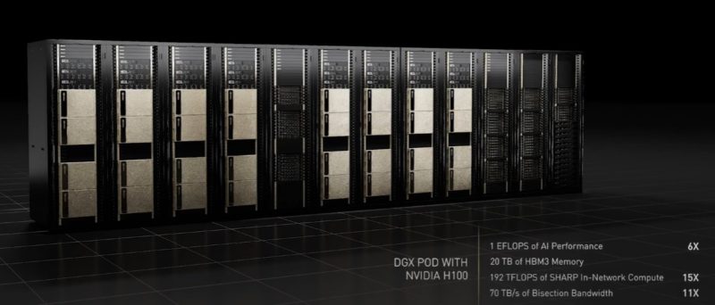
NVIDIA is really working on becoming a full-stack systems company like Apple, but for massive scale systems. Here are the stats on the DGX POD.
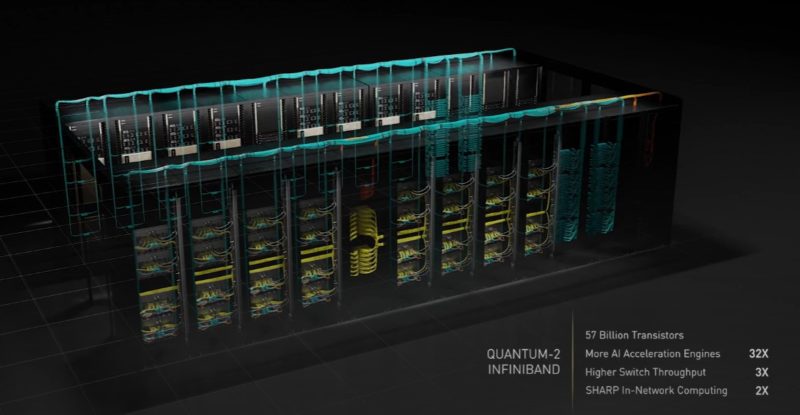
NVIDIA also uses Quantum-2 Infiniband.
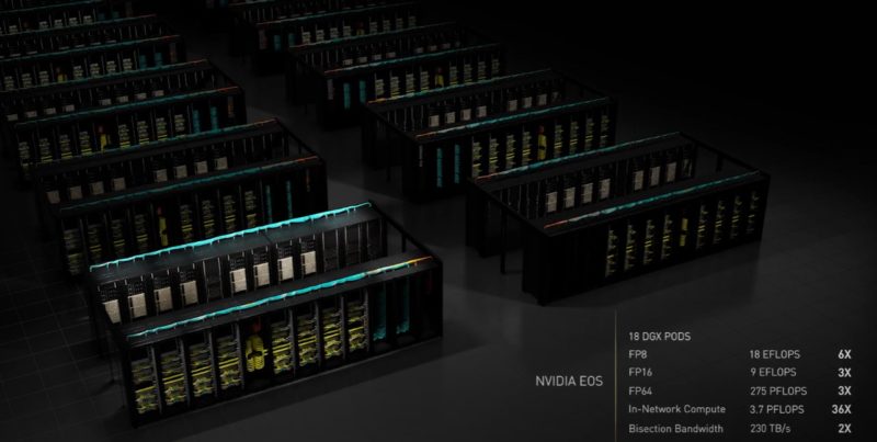
NVIDIA is building a massive supercomputer with NVIDIA Eos.
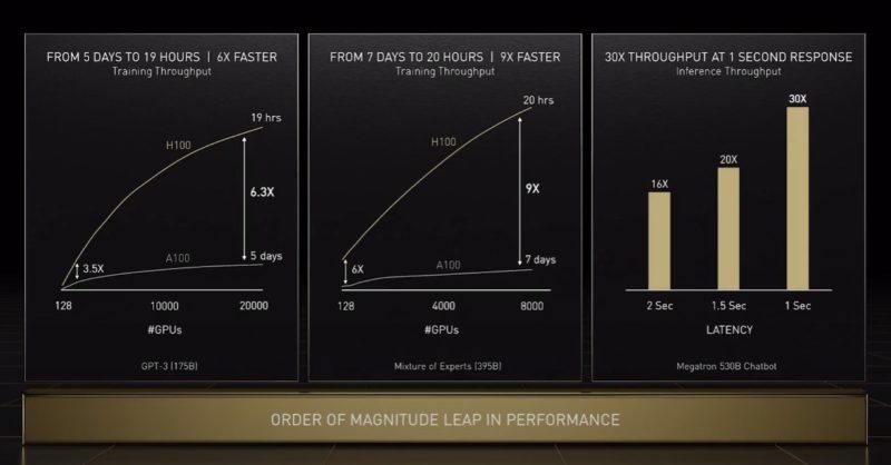
Here is a performance look at Hopper, but we will have more on this as we can.
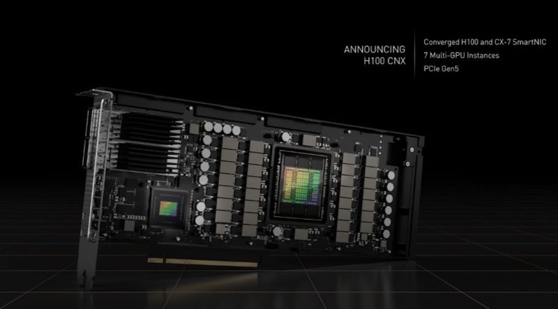
For PCIe servers, the NVIDIA H100 CNX will combine ConnectX-7 and the H100 onto a PCIe Gen5 card so that the GPU can have direct NIC access. NVIDIA has MHA and PCIe switch capabilities and that is how we think they are doing this. Also, we asked and this is a 350W TDP PCIe GPU like the standard H100 PCIe card will be. That is a massive TDP that many servers will not be able to cool.
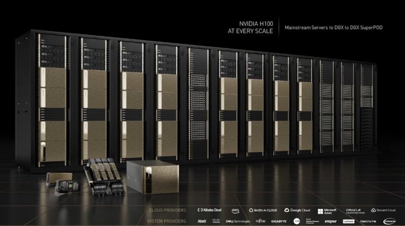
Here is the family:
Now onto perhaps the biggest announcement, Grace.
NVIDIA Grace Hopper Era for 2023
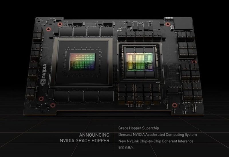
First, the NVIDIA Grace Hopper. This has a 900GB/s interface and has the GPU and CPU on one module.
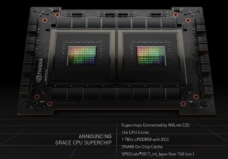
The new one for this year’s GTC is the Grace CPU Superchip. This takes two of the Arm CPU modules so we get 144 cores with 396MB of cache and 1TB/s of LPDDR5X memory bandwidth.
We heard about this one, but the big reveal is also in the middle of this slide. NVIDIA has a Grace CPU plus two Hoppers on a single module.
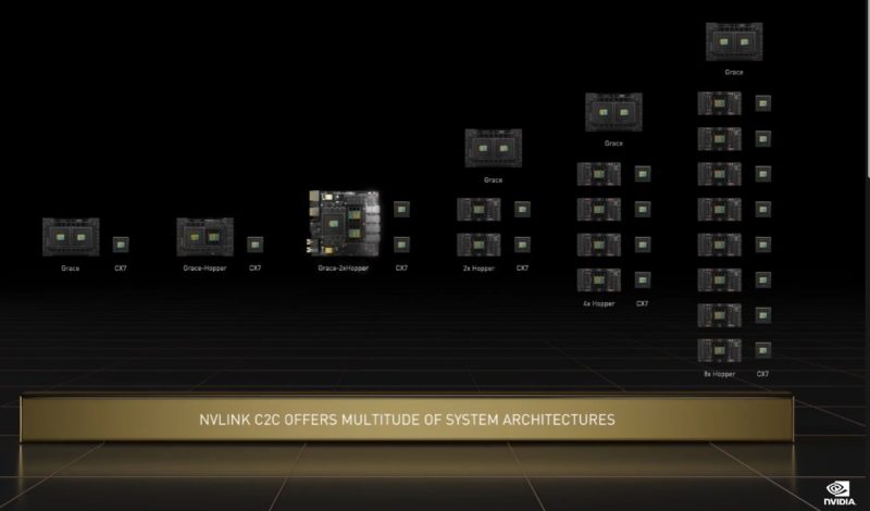
NVIDIA is using NVLink as the high-speed cache coherent interconnect. NVIDIA is also opening up NVLink for semi-custom chips.
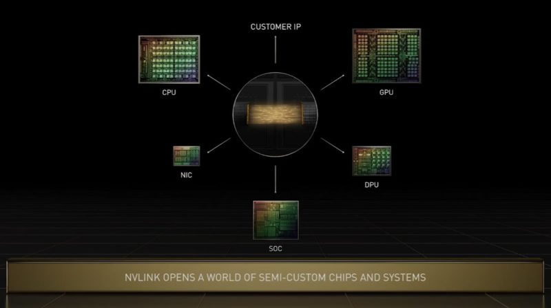
It will be interesting to see customer wins here, but when we talk about things like hyper-scalers pushing Universal Chiplet Interconnect Express UCIe 1.0 Launched, the idea of co-packaging IP from different vendors is becoming more mainstream. NVIDIA is pushing its technology into this space.
NVIDIA cuQuantum
NVIDIA cuQuantum is really interesting, the company has the ability to simulate/ emulate quantum machines on NVIDIA A100 GPUs.
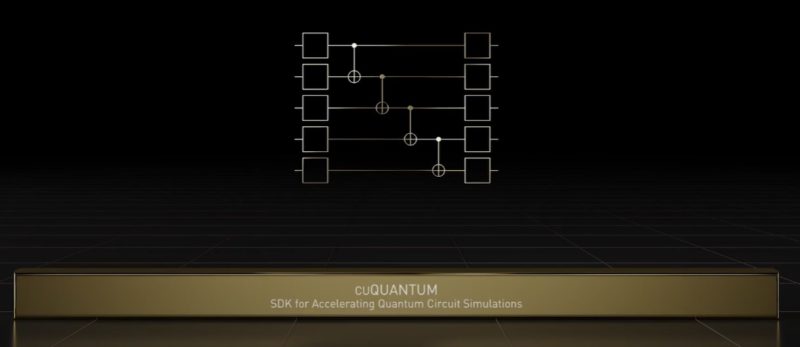
This is an announcement that only got a few moments in the GTC keynote, but there is a lot more happening. The company has a quantum compiler called nvq++ for the Quantum Intermediate Representation or QIR. This basically allows for a few things. First, it allows NVIDIA to work with a range of partners on quantum while the industry is still relatively young. It also allows NVIDIA to have researchers port code that can take advantage of quantum and make that part of overall simulations.

In a pre-briefing, I was told that the best people to program a quantum supercomputer today are quantum physicists. To get quantum more used and useful, that needs to come down to the domain practitioner level. Basically, you want the weather simulation expert making a weather simulation program instead of a quantum physicist. This all runs on DGX A100’s.
NVIDIA OVX Server
NVIDIA Omniverse is a huge effort at NVIDIA. Behind Omniverse, NVIDIA’s goal is to have companies create digital twins of just about everything. This can be cars, factories, kitchens, homes, or everyday products. This is the type of large-scale engineering problem, like AI, that if NVIDIA gets ingrained in, it becomes the ecosystem provider for. To that end, it is starting to make appliances for Omniverse, it calls OVX.
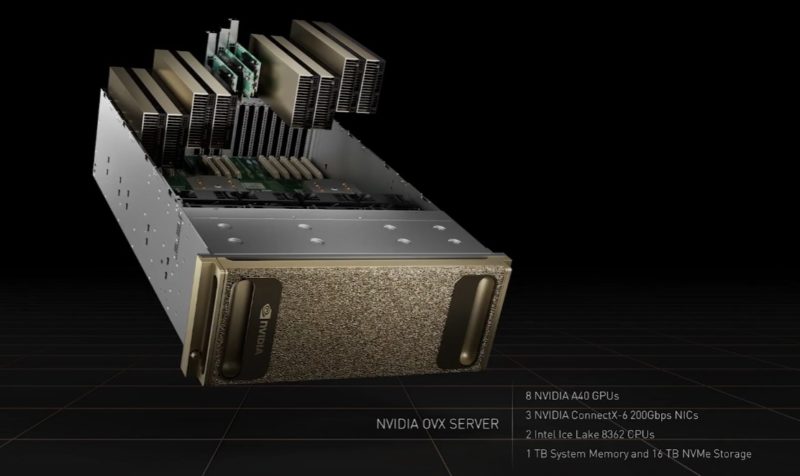
The first NVIDIA OVX server has 8x NVIDIA A40 GPUs. We just had our NVIDIA A40 48GB GPU Mini-Review. This is along with three ConnectX-6 NICs, two Intel Xeon Platinum 8362 CPUs like we used in our Deep Dive into Lowering Server Power Consumption piece. There is also 0.5TB of RAM per CPU for 1TB total and 16TB of NVMe storage in what looks like a 4U box.
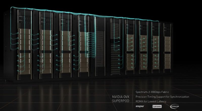
Combining this with the NVIDIA Spectrum 3 networking and precision time, we get a scale-out Omniverse pod.
NVIDIA Spectrum 4 400GbE/ 800GbE Switch Platform
NVIDIA has a new 51.2T switch that it has announced called the Spectrum-4. This has 12.8T of crypto and is using 100G-class SerDes.
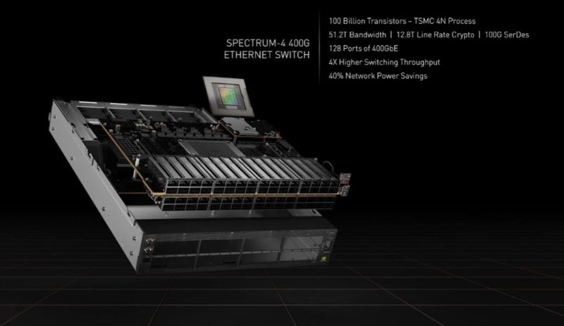
While this is exciting, it is sampling in late Q4 2022. Sampling in late Q4 2022 means that this will likely be GA sometime in 2023.
Autonomous Vehicles with NVIDIA Drive Hyperion 9 and Atlan AV SoC
NVIDIA is announcing many partnerships in the automaker industry for autonomous cars. One of the big announcements is the Hyperion 9 platform and its dual Atlan AV SoC computer.
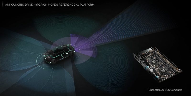
This will handle more sensors to help add more capabilities into cars. Something that is really interesting here is that automakers are moving to a model where there will be major new platforms on a regular basis. Automakers typically have very long design cycles, so these are platforms for several years in the future, well before NVIDIA can actually make the parts.
NVIDIA Jetson AGX Orin
Along with automobiles and the Omniverse vision of digital twins, NVIDIA has its robotics platform the Isaac Nova upgraded as well.
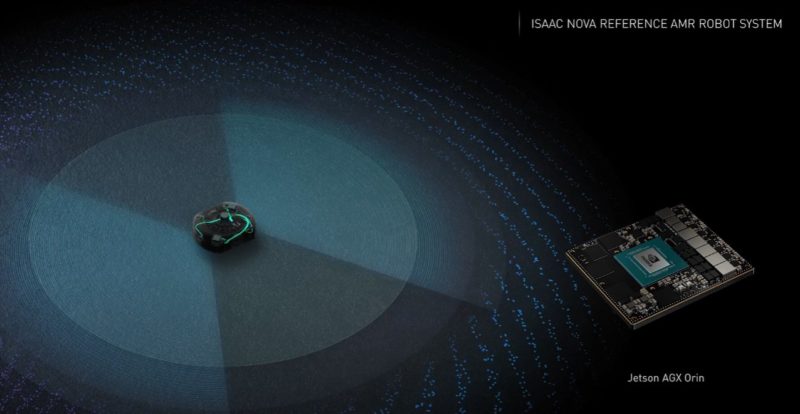
NVIDIA Jetson AGX Orin developer kits are available today. These are new kits that offer big spec improvements and new GPU IP.
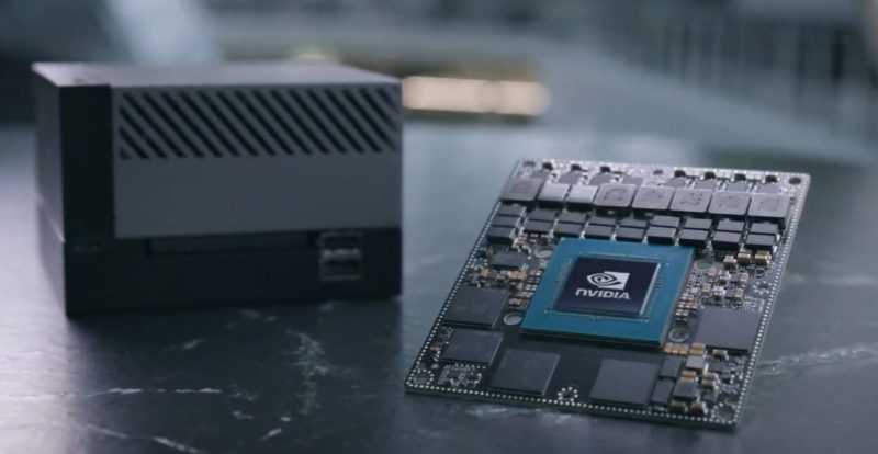
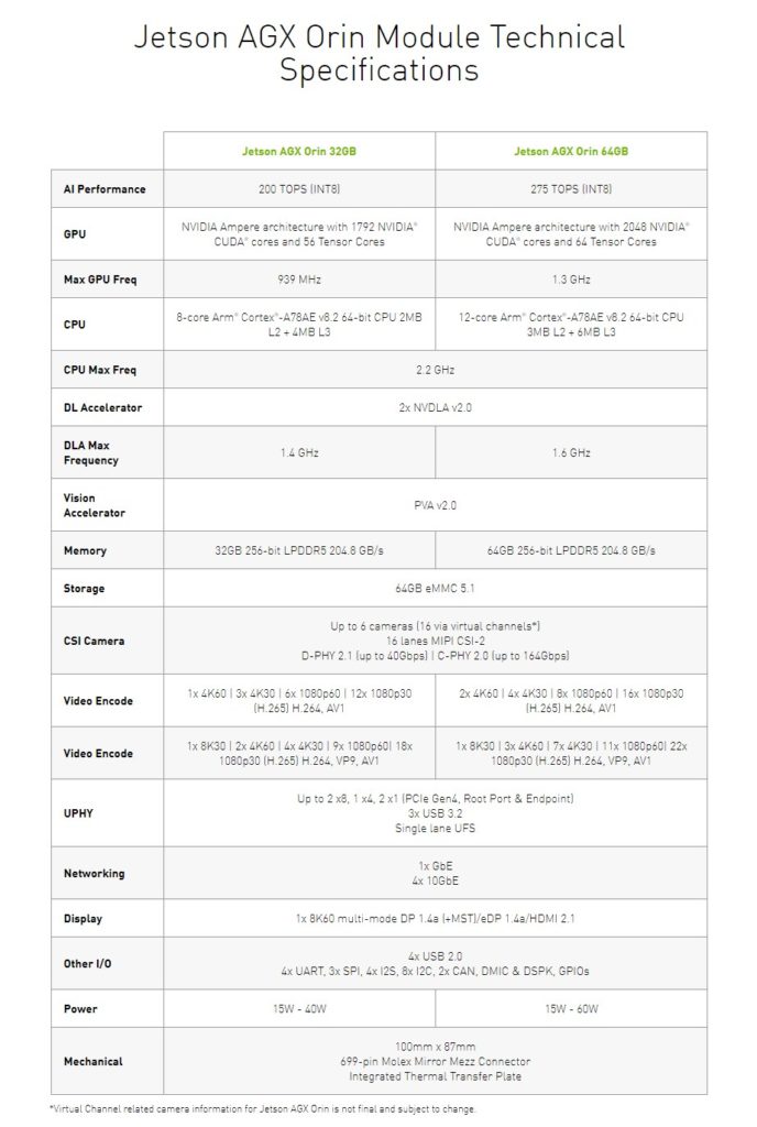
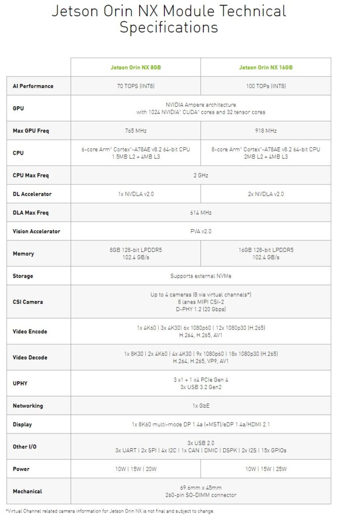
The new Orin modules will come in both the larger form factor with 32GB or 64GB of memory and the NX form factor with 8GB or 16GB.
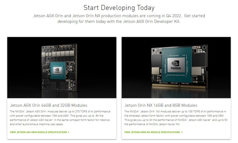
Here are the specs for the larger modules, bringing Ampere to the Jetson line:
Here are the specs for the NX version. It is not just the memory capacity changing, we can also see clock speeds, core counts, and accelerators changing.
NVIDIA says they are available now, but we cannot figure out where to get the kits.
Final Words
Finally, NVIDIA’s outro was a dancing data center.
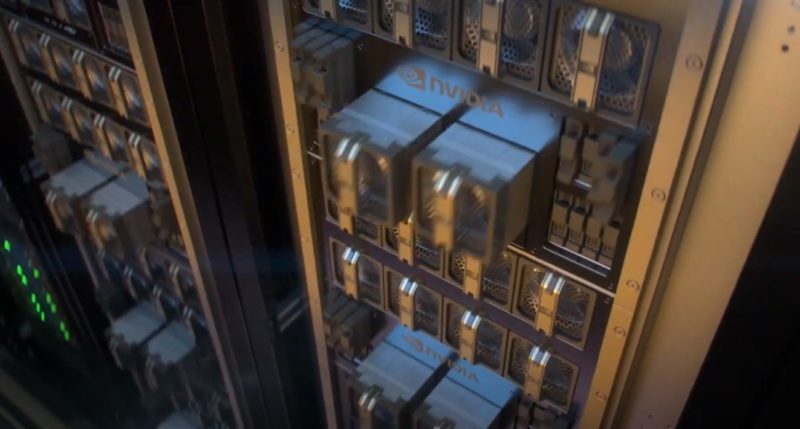
I have no idea what was going on, but I appreciated it.
For some perspective, the announcements today of the Hopper H100, many of the networking innovations, and so forth are not products available after the show. They are very much forward-looking to the products we will see, and hear more about later this year. My best sense is that we are going to start seeing Hopper in the second half of the year and then Grace in 2023 with a roll-out of different models. Still, there is a lot of cool technology coming. If you follow STH, you now have a better glimpse into why I am excited for the next few years.
NVIDIA GeForce RTX 3080 Ti Giveaway for GTC
NVIDIA is sponsoring a GPU giveaway on STH for GTC 2022. For this, you likely need to have a free GTC 2022 account. If you do not already have one, you can register on the GTC website. Registration is free this year and there are hundreds of free sessions. Then take a screenshot, uploading it below with a quick caption as to why the session is your favorite.
Here is the simple giveaway form:
For those who want a few bonus entries, after you submit the photo, you can get a bonus entry by subscribing to the STH Newsletter and/or going to the NVIDIA GTC 2022 page again.


“…a full-stack systems company like Apple.”
Wut?
Been hitting refresh to see if this is a mistake :(
https://developer.nvidia.com/buy-jetson?product=jetson_agx_orin&location=US
“Jetson AGX Orin Developer Kit is not available for purchase in United States.”
Conflicting information during the GTC presentation:
Is the H100 4.9TB/s memory bandwidth or 3TB/s(3*8=24TB/s)? According to Anandtech, it is 3TB/s, which is a bummer if true, only 50% higher than A100
Have to wait a bit to see what the actual parts come in at.
@Patrick:
Thought about it for about half a day, and realized the following:
The chip was probably designed for 4.9TB/s max(6 stacks of 819GB/sec HBM3 specification), but nvidia probably couldn’t fit 6 stacks of 819GB/s HBM3 into the 700W SXM5 socket TDP limitation, so nvidia took the easy way out and got 6 stacks at 600GB/s with 1 stack either disabled or for “RAID5” purposes for a total of 3TB/s usable.
The real question is this: with only 50% more memory bandwidth than a100, how did Nvidia manage to fit 60TF of Double Precision(3x boost compared to a100, and the rest of the specs are also across the board 3x?) The DP 3x boost is questionable, because it couldn’t be cheated on like having TF32 format reducing 32bits to 19bits.
Another thing is this: if the 700W SXM5 could only do 3TB/s, the 350w PCIe will probably do 2TB/s, and would have the same memory bandwidth as SXM4 A100s, and how much cut in performance will that incur?
I think Nvidia’s H100 chip is design ready at 4.9TB/s, HBM3 wasn’t, and we will probably have to wait for a HBM3 die shrink for both capacity and TDP improvement before we will see 4.9TB/s H100 SXM5 to land? I mean 3TB/s and 4.9TB/s is a generational leap.
Moore’s Law is dead just leaked the DP number:
*Vector* Double Precision = 30TF! 50% Higher than A100, which now is the right number corresponding to exactly the 50% higher HBM3 bandwidth
*Matrix* Double Precision = 60TF, basically the same Tensor Fake Teraflops you should ignore
It’s sad that Nvidia is using 3TB+0.9TB+0.9TB+0.128TB to get to the 4.9TB, looks like H100 would be a transformer-only solution for now.
TS – updated with how NVIDIA came up with 4.9TB/s
Actually, A100 has 9.7TF of FP64 non tensor, so 30TF (which was available at the whitepaper at presentation of Hopper) is 3X from A100