There is quite a bit of confusion online about NVIDIA’s Grace parts. These Arm Neoverse V2-based parts are a major part of NVIDIA’s push beyond accelerators into mainstream data center computing. One major myth we have heard is that the 72-core plus NVIDIA H100 Grace Hopper (GH200) and the 144-core NVIDIA Grace Superchip can be used in the same servers. The myth is that a server that accepts one accepts the other. They cannot because they are not compatible.
NVIDIA Grace Hopper GH200 and Grace Superchip Pictured and Incompatible
Here are the two parts side by side. On the left, we have the NVIDIA Grace Hopper GH200. This module has the H100 on the top spot and the 72-core Arm Neoverse V2 Grace chip on the bottom, flanked by memory packages. On the right, we see two of these NVIDIA Grace chips with twice as many memory packages. Immediately one may notice that the cutouts on the PCB edges are a bit different, but that is far from the only difference.
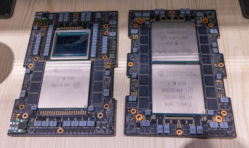
Looking at the bottom, we can see that the GH200 has LPDDR5X modules on the half of the board with the Grace Arm CPU. The Grace Superchip has sixteen LPDDR5X modules spanning the full module, eight for each Arm CPU onboard. That brings us to sixteen LPDDDR5X packages for each CPU when we add them to the packages on the front.
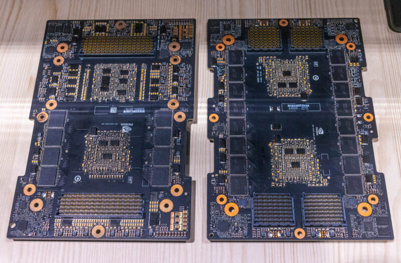
From the compatibility angle, we can see that the GH200 and the Grace Superchip have different connectors on the bottom. These connectors are used to connect the modules to their host boards. The impact of this is significant, but it makes sense. There is a different amount of I/O and power requirements for the two parts, so we would expect there to bem at minimum, signaling differences. NVIDIA’s approach is not to make these parts swappable, where one can use the same base PCB and have either the GH200 or Grace Superchip. Instead, the base carrier board and the NVIDIA module must be matched.
Final Words
There are many in the industry who saw similarly sized modules, both having at least one 72-core Grace CPU, and thought that the same server could be used by just swapping the two types of modules. Hopefully, these photos illustrate why that is not the case since the connectors between the NVIDIA modules and the carrier boards are different.
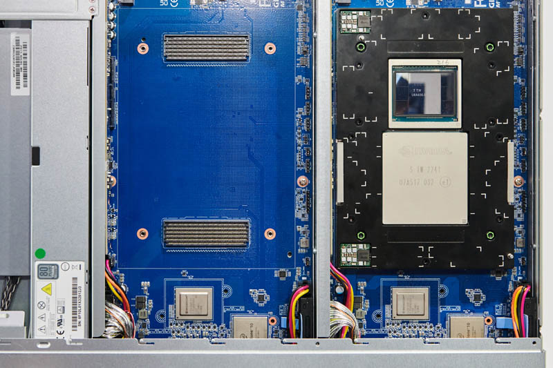
To us, the more perplexing part is why NVIDIA does not sell a standardized half-width carrier board with each of these with MCIO connectivity for the PCIe lanes and standard power inputs. We have seen a number of NVIDIA MGX designs already and many are very similar. MGX has the effect of minimizing the importance of OEMs in many cases, so it seems strange that NVIDIA does not sell the entire assembly as it does with Delta-Next and Redstone-Next platforms.



you know what
the techfans in China will call such pictures “赛博色图” which means “cyber porn pictures”
pictures above are very attractive for techfans
Indeed why not go with a blade scheme with the IO on a backplane. It would be more dense.
Another thing – “Superchip”. How does it stack up to a 64 or 96 core AMD Epyc or 56 core Intel Xeon? Is it actually super?
Too bad the author can’t spell… Should say ‘ARE’ incompatible… not ‘AND’.