The NVIDIA DGX A100 is the company’s new 8x GPU flagship system. In many ways, this is the successor to the Inspur NF5488M5 Review A Unique 8x NVIDIA Tesla V100 Server we reviewed. The solution integrates 8x NVIDIA A100 SXM3 GPUs onto a HGX PCB that is wrapped by all of the CPUs, memory, and networking that one may need. A major reason we agreed to do that late-cycle Tesla V100 GPU system is because it mirrors the new DGX A100 design in several ways. The DGX A100 is set to leapfrog the previous generation DGX-1 and even the DGX-2 for many reasons.
NVIDIA DGX A100 Overview
The NVIDIA DGX A100 is a fully-integrated system from NVIDIA. The solution includes GPUs, internal (NVLink) and external (Infiniband/ Ethernet) fabrics, dual CPUs, memory, NVMe storage, all in a single chassis.
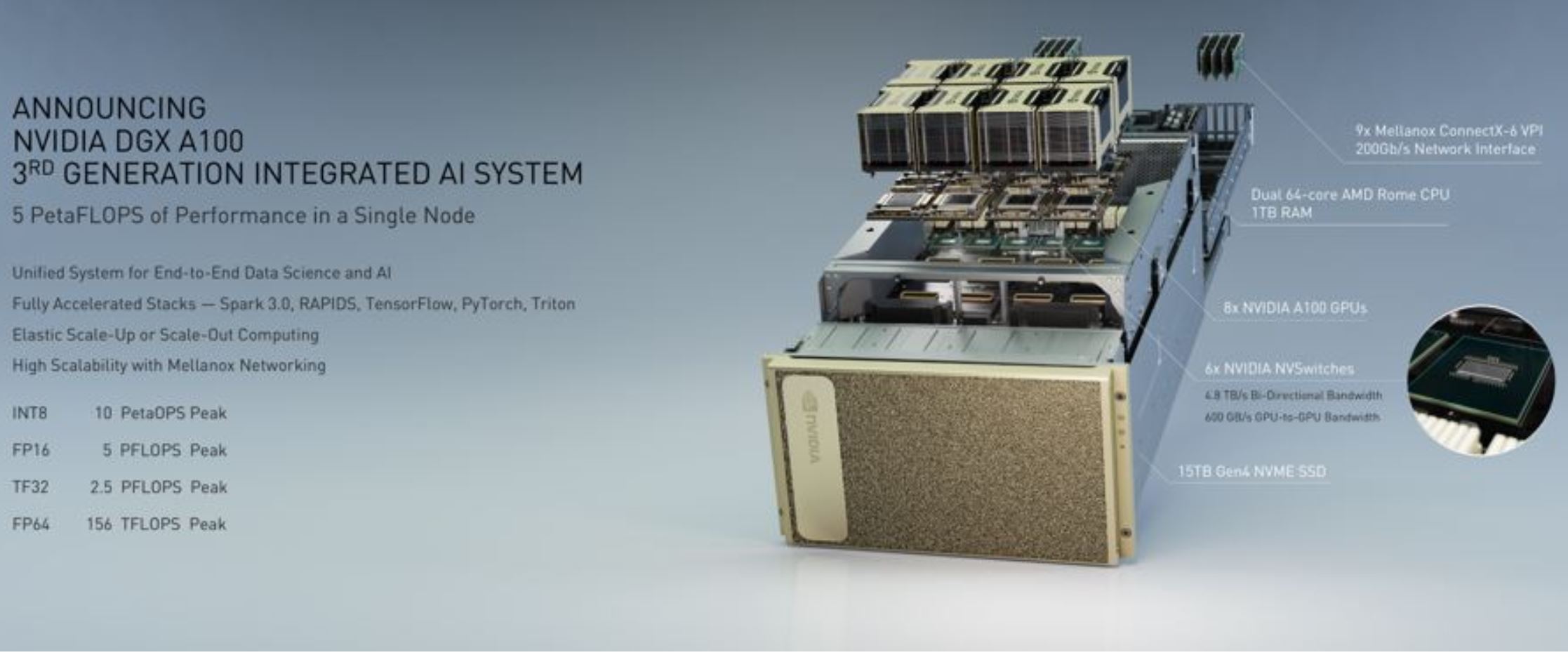
Here are the main highlights from the machine:
- 8x NVIDIA A100 Tensor Core GPUs, delivering 5 petaflops of AI power, with 320GB in
total GPU memory with 12.4TB per second in bandwidth. - 6x NVIDIA NVSwitch interconnect fabrics with third-generation NVIDIA NVLink
technology for 4.8TB per second of bi-directional bandwidth. - 9x Mellanox ConnectX-6 HDR 200Gb per second network interfaces, offering a total of
3.6Tb per second of bi-directional bandwidth. - Mellanox In-Network Computing and network acceleration engines such as RDMA,
GPUDirect and Scalable Hierarchical Aggregation and Reduction Protocol (SHARP) - 15TB Gen4 NVMe internal storage, which is 2x faster than Gen3 NVMe SSDs. The DGX A100 uses 2x 1.92TB NVMe SSDs for OS and 4x 3.84TB internal NVMe SSDs for local storage.
- Two 64-core AMD EPYC 7742 “Rome” Processors
- 1TB of RAM
- NVIDIA DGX software stack
Just as a quick note here, since the system uses NVSwitch, there is actually a distinct software stack as we saw in our recent review. That “DGX software stack” includes frameworks and acceleration, but also dedicated monitoring and management tools for the NVSwitch fabric.
The system itself is an 8x GPU unit, but NVIDIA argues that with the new A100 GPUs, it is faster than the HGX-2 and at a lower power per unit of compute.
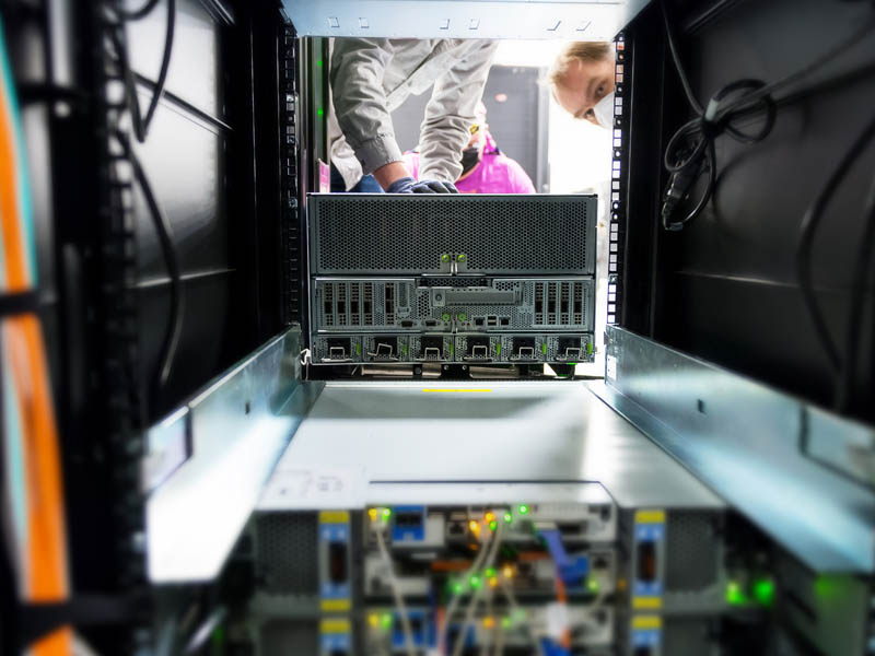
One of the really interesting departures here is that NVIDIA went with AMD EPYC 7002 “Rome” CPUs. NVIDIA wanted PCIe Gen4 and Intel cannot offer it with Xeon so NVIDIA is sourcing CPUs from its (current) chief GPU competitor AMD. Here is the quick overview video NVIDIA has:
For AMD, this is actually a huge win. This is now the gold standard in deep learning machines and it is based on Rome because of the PCIe Gen4 platform feature. What is not mentioned in the release is that the system is also using PCIe Gen4 switches onboard. This is part of the SXM3-based HGX designs.
NVIDIA HGX A100 Building Block
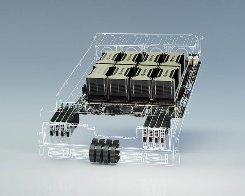
The NVIDIA HGX A100 (codenamed “Delta”) is the building block for the entire server. This utilizes eight NVIDIA A100 GPUs, six second-gen NVSwitches, as well as eight Mellanox fabric adapters. The smaller 4x GPU building block is codenamed “Redstone” as a lower-cost option. This HGX A100 platform is what NVIDIA and other server vendors will use to create their versions of the DGX A100.
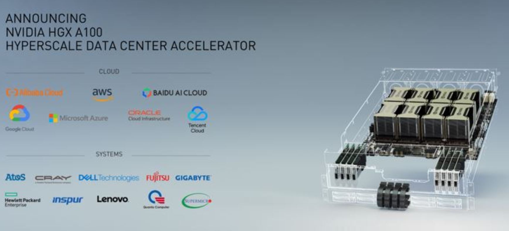
NVIDIA is claiming several major customers as part of this. Effectively, all of the big players except one are deploying this. The one obvious exception here is Facebook. Facebook has effectively become an all-in on Intel shop likely prompting the Intel – Habana Labs acquisition.
If you want to see an example of how the HGX platform can be integrated into an 8x GPU server, you can check out our Tesla V100 video as well where we show many of the key HGX PCB components.
The HGX platform is designed for NVIDIA A100 GPUs. Each GPU is fully connected due to the NVSwitch fabric. That gives each GPU up to 600GB/s of GPU-to-GPU bandwidth. Each GPU now has 12 NVLinks up from 6 in the previous generation which doubles bandwidth.
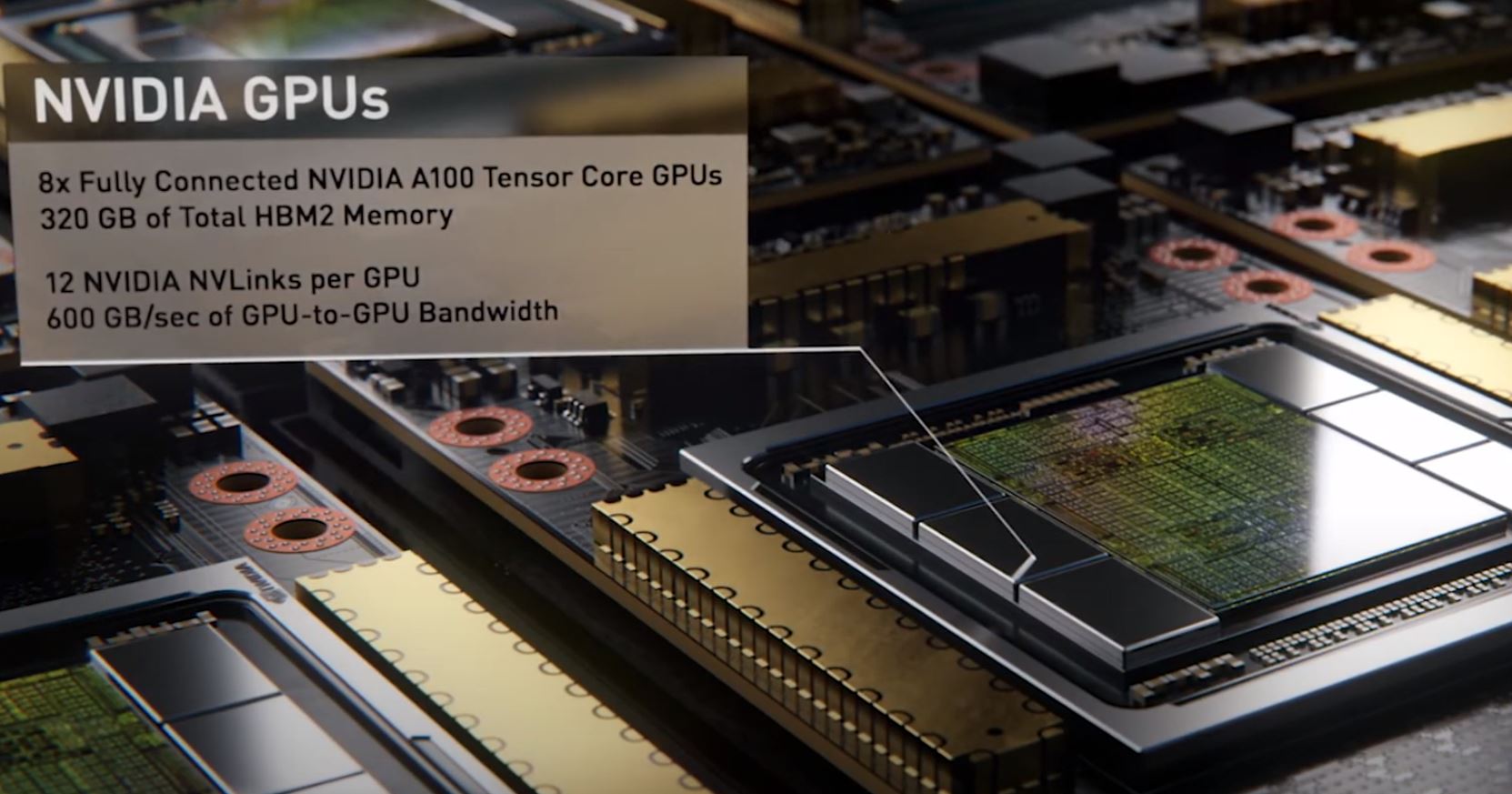
There are a total of 8x A100 GPUs onboard. They come pre-installed on the HGX motherboard. With this, NVIDIA can sell complete solutions to its customers that are easier to integrate.
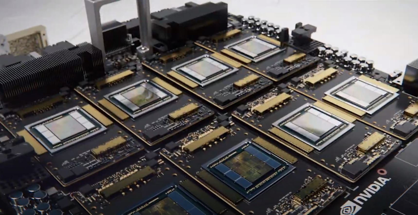
There are six NVSwitches on the HGX platform. Each NVSwitch gets 2 links to each GPU which gives 12 links total. Each GPU can transfer data to any other GPU using two links through each switch across six switches. That is how NVIDIA is getting so much bandwidth. You can read more in our NVIDIA NVSwitch Details at Hot Chips 30. This is a big upgrade compared to how they were used in the Tesla V100 generation.
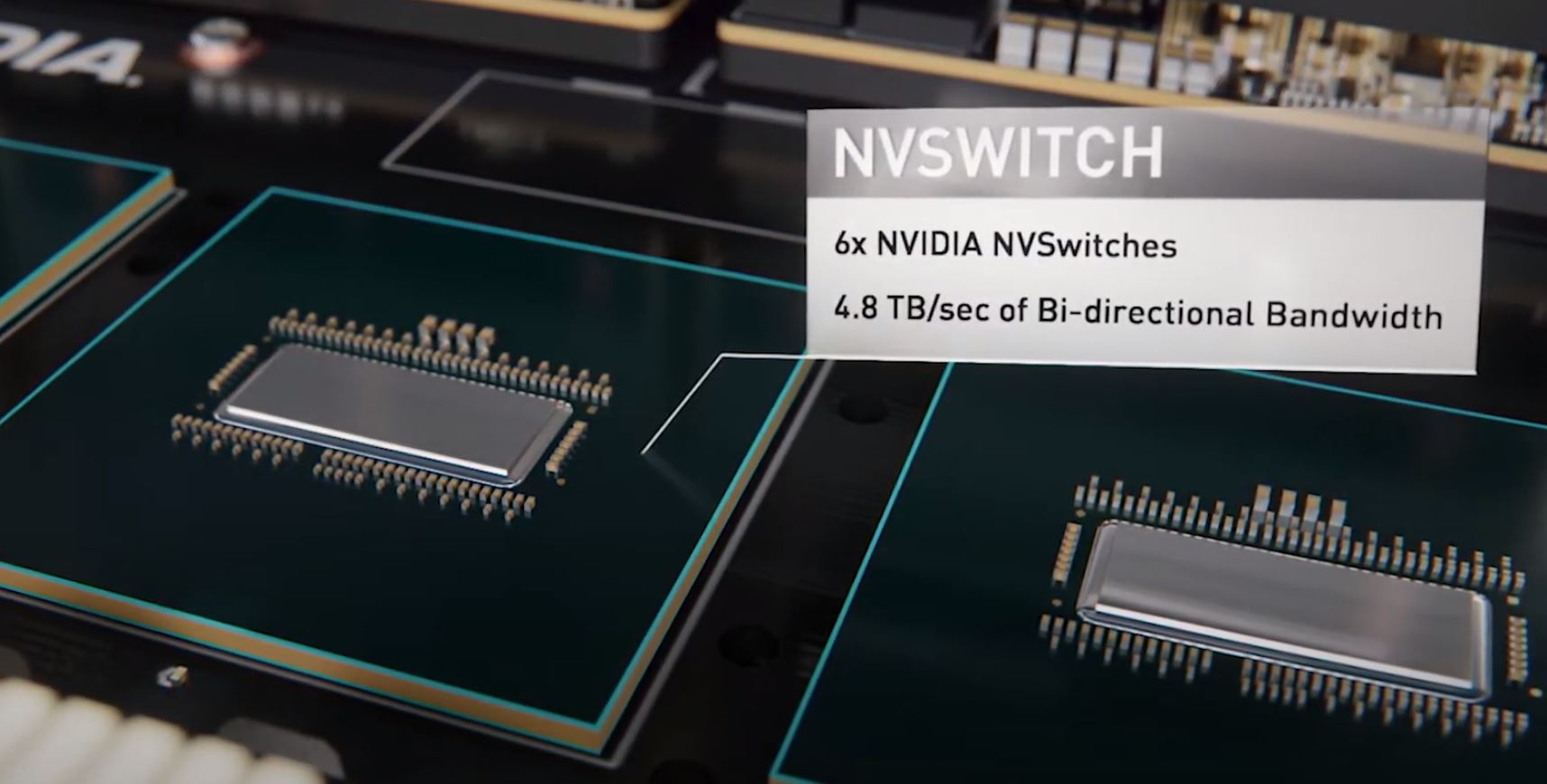
One quick item to note here is that the NVSwitch architecture is all within a single 8x GPU HGX board here. If you saw our NVIDIA DGX-2 Details at Hot Chips 30 you can see that with the 16x GPU DGX-2 we had HGX board to HGX board NVLink between the NVSwitches. Now, those lanes, plus likely some of the reserved lanes are being used to service the extra NVLink lanes on the A100 GPUs.
Each NVIDIA A100 gets access to a dedicated Mellanox ConnectX-6 VPI card. VPI means the card can run either Ethernet or Infiniband fabrics. In previous DGX designs the ratio was one NIC to two GPUs. Now with the NVIDIA-Mellanox Acquisition, we get twice as many cards. Each card can handle 200Gbps networking due to a PCIe Gen4 x16 interface. PCIe Gen3 cannot handle 200Gbps in a x16 slot.
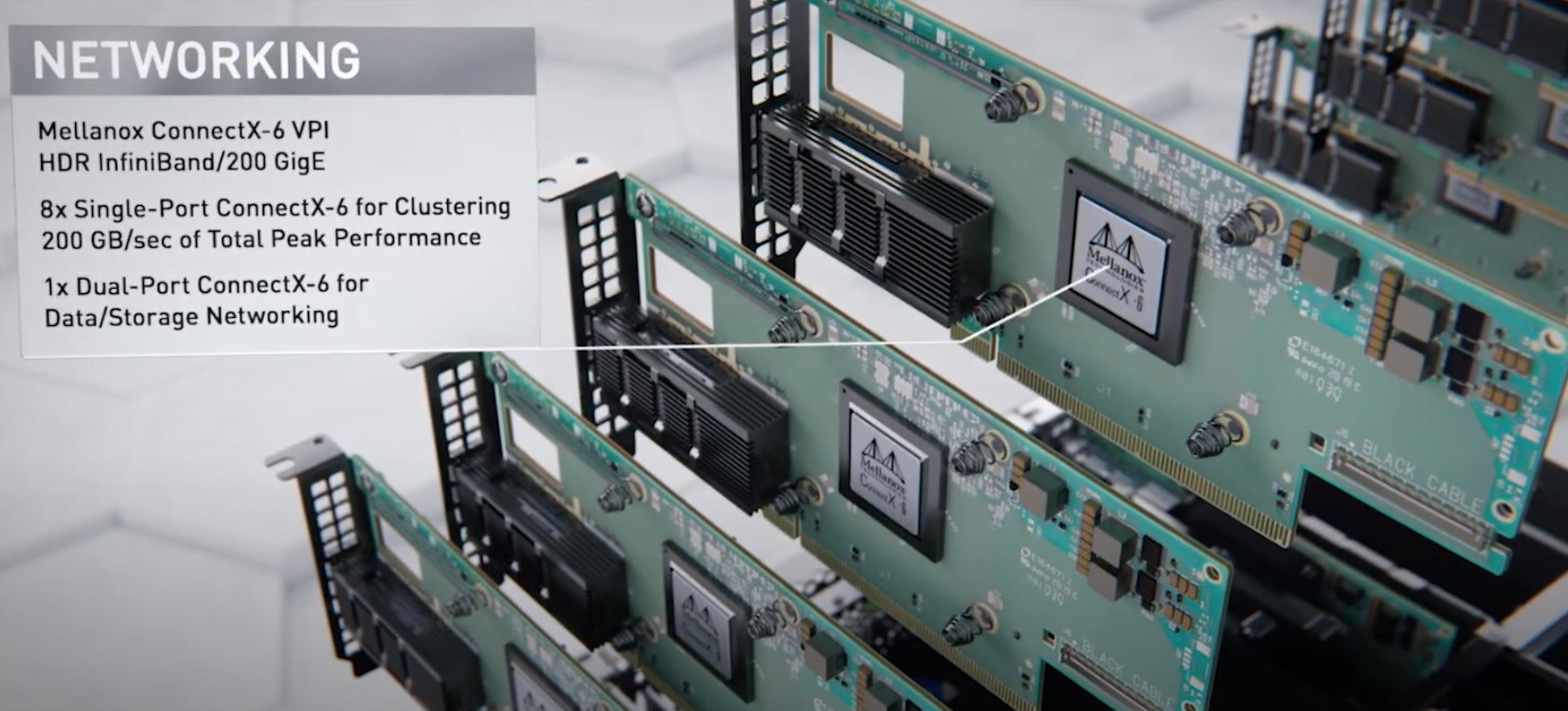
There is also another dual-port ConnectX-6 card for storage and networking. Overall, there is around 1.8Tbps of external network connectivity in a DGX A100 and HGX A100 platform.
The Broader Mellanox Integration Story
Beyond the single $199K NVIDIA DGX A100, NVIDIA is thinking bigger. It is creating a pre-validated solution with 140x DGX A100 systems and 170x Mellanox Quantum 200G Infiniband switches to deliver an easy to spec and deploy cluster. Effectively, with the DGX A100 SuperPOD NVIDIA moving into space many bespoke HPC cluster VARs previously played in.
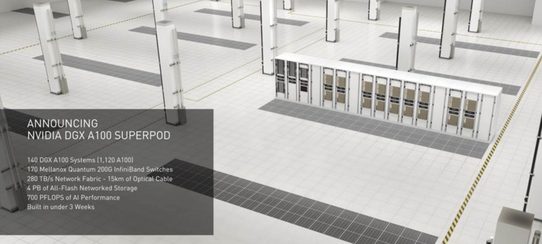
NVIDIA says it is adding four DGX SuperPODs to its SaturnV cluster.
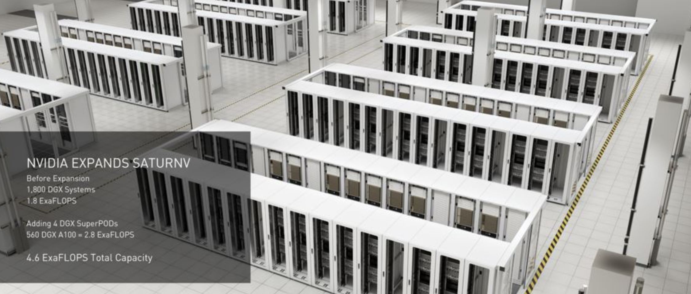
For some customers, this may be an easy way to get a new cluster running. Still, one of these clusters will cost tens of millions of dollars so it is likely that these will be customized for intended customers. Even a reasonably well-funded and mature AI startup will not be able to afford something like this, however large enterprises and government organizations can. There is almost always a segment that wants turnkey simplicity.
Final Words
A common theme for the GTC 2020 keynote is the integration of Mellanox and NVIDIA. The $199K DGX A100 certainly delivers on that message along with eight of the highest-end GPUs one can buy right now. In the near future, if you are not an extremely large customer, the DGX A100 is likely your best bet to get Ampere quickly.
Overall, we are going to see many more partner systems that take the HGX A100 building block at the heart of the DGX A100 and integrate it into systems designed for different markets.
Note: We got late word that this is now the NVIDIA A100 without the “Tesla” branding.

I might be able to see a point when our 2 in-house DGX-2 (16x Volta 350W) are replaced with 2 8xAmpere systems. The 24KW power draw is the biggest concern on the current units. If I can get the same perf/throughput, then it would be a no brainer. However, with 2 DGX A100 (16x Ampere per), we can keep the same time required for certain workloads and increase fidelity – much as we did when we moved from the Pascal units to Volta.