AMD heard the feedback that many wanted a bit more on the new AMD Ryzen AI 300 series, Ryzen 9000 CPUs, and Zen 5, and so we have some more to share. That includes functional block diagrams, a few PCIe lane changes, and even areas the Zen 5 cores improved. Let us get into it quickly.
AMD Zen 5 and Zen 5c Optimization
Something cool that we got from AMD this week was the Zen 4 to Zen 5 comparison. We will have some detailed slides below, but this is a great summary of what changes in the processor impacted the Zen 5 performance.
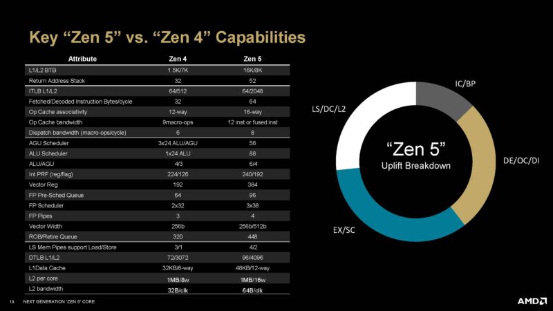
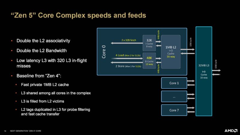
Here is a bit more on the Zen 5 speeds and feeds and why this processor is faster than Zen 4.
Here are the new Zen 5 ISA improvements and instructions:
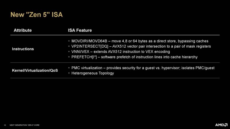
The PREFETCH[I*] is to help prefetch into the ICache. Previously, AMD had a better way to do this into the DCache.
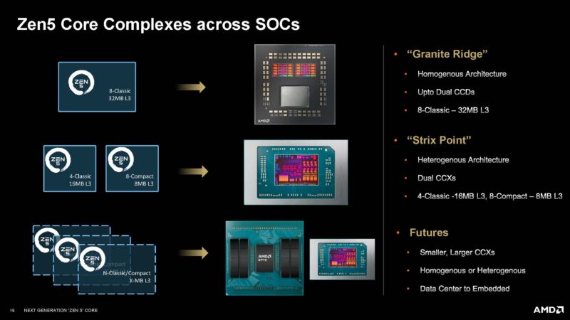
With the AMD Ryzen AI 300 series, we have heterogeneous Zen 5 and Zen 5c cores. Zen 5c trades off a smaller L3 cache and top-end frequency for better power efficiency.
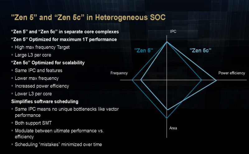
That heterogeneous SoC is relevant in the context of the AMD Ryzen AI 300 series.
AMD Ryzen AI 300 Series Update
AMD sent this Strix Point SoC diagram. Here, we can see some details from our previous piece, including how the Zen 5 and Zen 5c complexes need to go through the on-chip fabric to reach the other cluster’s L3 cache.
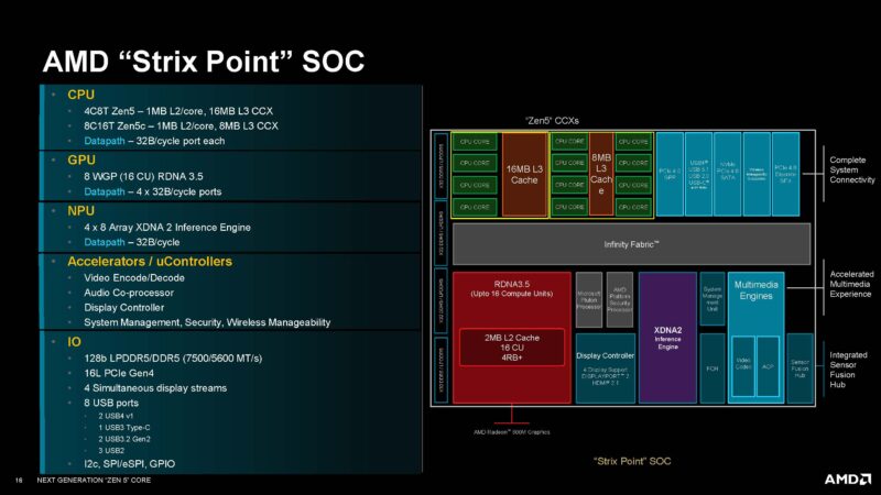
One of the more interesting points AMD made was that the PCIe lanes are down from 20 to 16. Apparently, the attach rate of utilizing those extra lanes was not high. The common use case was adding another M.2 SSD, but that was infrequently used.
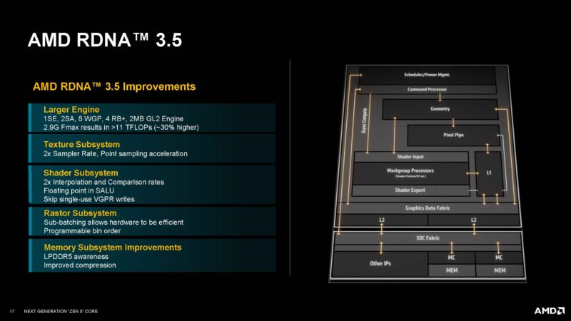
In our previous Architecture Trifecta AMD Zen 5 RDNA 3.5 and XDNA 2 piece, we discussed the new integrated GPU. AMD said that while they leveraged learning from the mobile IP licensing business, the bulk of the performance comes from building a larger engine.
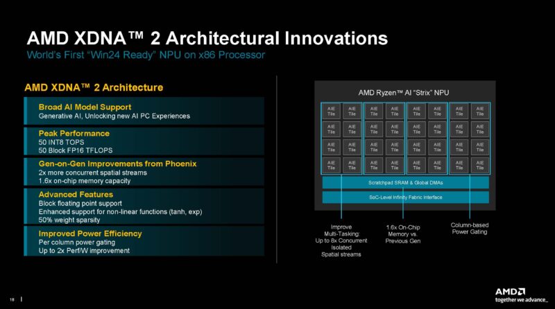
Here is the slide on XDNA 2 again:
Next, let us get to the AMD Ryzen 9000 series.
AMD Ryzen 9000 Series Update
The AMD Ryzen 9000 series SoC utilizes homogeneous Zen 5 core complexes. At the same time, not everything is new. It appears as though AMD recycled the previous generation I/O die.
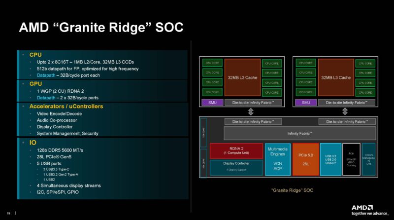
As such, we are going to expect the AMD Ryzen 9000 series to mostly be helped by the Zen 5 improvements, so next we have the detail slides.
AMD Zen 5 Microarchitecture Update
We already showed the key levers AMD used to increase Zen 5 performance, but AMD went into a bit more details. One on this slide is that Zen 5 was designed for 4nm and 3nm process nodes.

Here is the block diagram of the Zen 5 core and the key overview items.
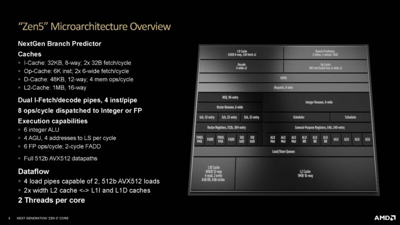
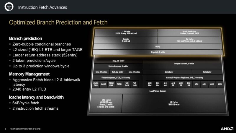
We are going to let folks read through the slides rather than repeating them. Here is the optimized branch prediction and fetch.
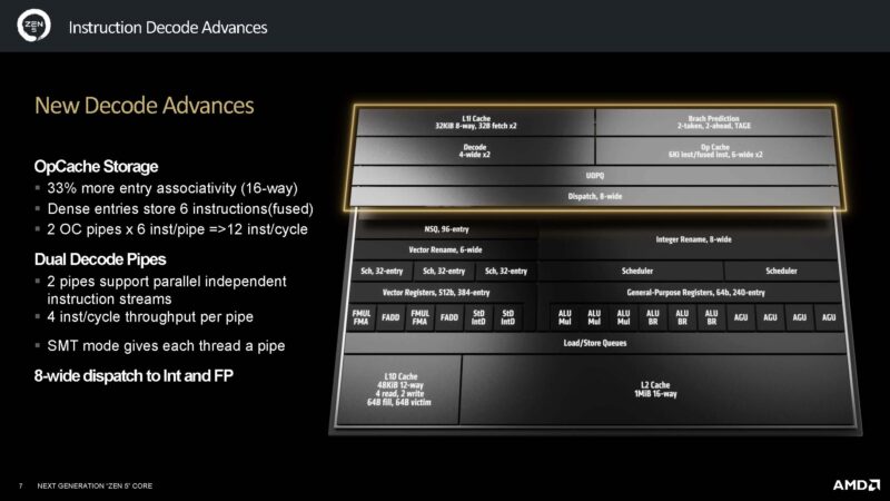
AMD has new OpCache storage, and dual decode pipes.
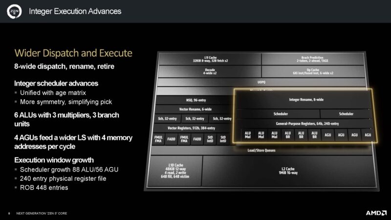
The dispatch has grown to 8 wide and has a bigger execution window.
AMD also spent a lot of time on increasing the bandwith within the cores.
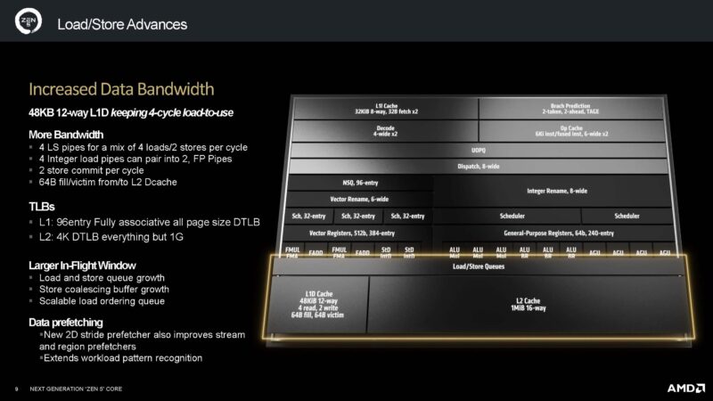
On the floating point side, perhaps the big one is that AMD has a new AVX512 with full 512b datapath.
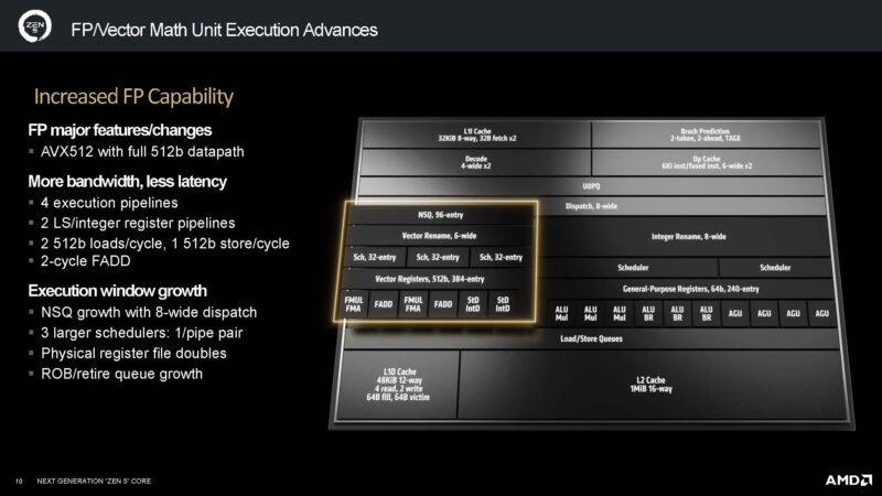
The company says it has figured out a way to feed the AVX512 engines without having to resort to dramatic clock speed reductions.
Final Words
Part of the reason we are showing this is becuase the AMD Ryzen 9000 series (and perhaps an update one day to the EPYC 4000 series?) and the Ryzen AI 300 series use the new cores. The other part is looking to the future with Turin and Turin Dense in Q4.
It will be interesting to see how AMD’s and Intel’s approaches to lower power cores emerge. For example, AMD calls SMT one of its most effective performance per watt tools. At least this year is shaping up to be a lot of fun on the CPU side.


I would like to see all OEMs utilize the integrated USB4 controllers, because they have no excuse not to, other than artificial market segmentation.
Typo in the PCI lanes section. Quoting:
“One of the more interesting points AMD made was that the PCIe lanes are down from 20 to 16. Apparently the attach rate of utilizing those extra lanes.”
I am not sure what is missing.
Otherwise good article, thanks!