
Kicking off Hot Chips 2026 Day 0, which has become a big day in itself, Micron is talking about evolving memory architectures for AI. From what it can tell, Micron will be walking through how high-bandwidth memory and advanced packaging have moved to the center of AI system design. Ok let us get started.
These are being done live, so please excuse typos.
Micron Evolving Memory Architectures for AI at Hot Chips 2026
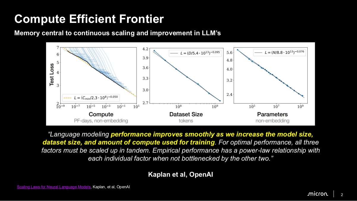
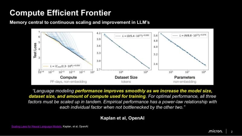
Micron’s talk opened with the OpenAI compute-efficient frontier to frame why memory has become central to language model scaling. Micron points to the power-law relationship between model size, dataset size, and training compute, arguing that all three must scale together for LLM performance to improve. Memory is the resource that ties those three factors together.
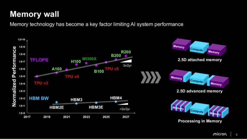
Now we are moving onto the memory wall. I wonder how many of these we are going to see today or even this week at Hot Chips! Micron is saying that AI accelerator TFLOPS roughly grow by 3x every two years while the bandwidth of 2.5D attached memory such as HBM climbs at under 2x per two years. That widening gap is why memory technology has become a key factor limiting AI system performance.
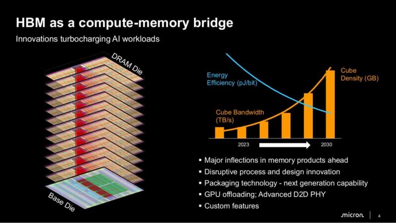
Micron frames HBM as the compute-memory bridge, tracking rising cube capacity, bandwidth, and energy efficiency across generations from HBM2e through HBM5. You have to enjoy the technical conference with unlabeled Y axis.
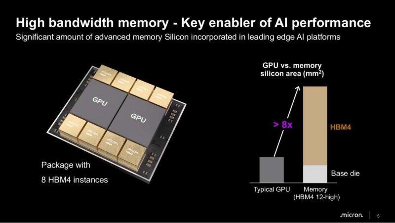
Here, Micron is showing a typical GPU at over 12,000 square millimeters when counting the package with base die and eight HBM4 instances, meaning memory silicon can exceed 8x the surface of the GPU die itself when using 12-high HBM4. This is actually a neat view to show
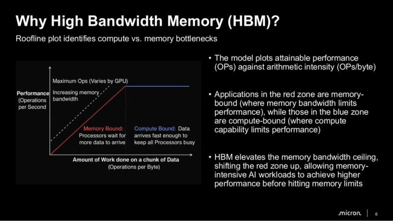
HBM raises the memory bandwidth ceiling, shifting that boundary and allowing memory-intensive AI workloads to run faster before they hit a memory limit.
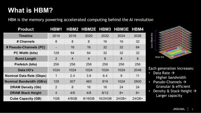
Micron’s talk is now walking through what HBM is and how each generation has advanced. A product table traces HBM1 through HBM4. Every generation increases data rate, pseudo-channels, and stack height, delivering higher bandwidth and larger capacity.
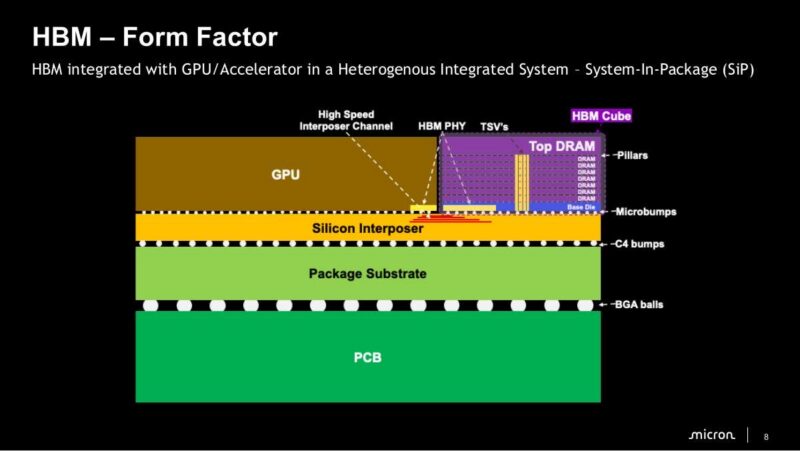
HBM does not mount like a standard ECC RDIMM. This figure shows how HBM stacks are integrated with the GPU or accelerator in a heterogeneous integrated system, packaged as a System-in-Package (SiP) rather than a separate socketed module. I think many at STH will have seen this before.
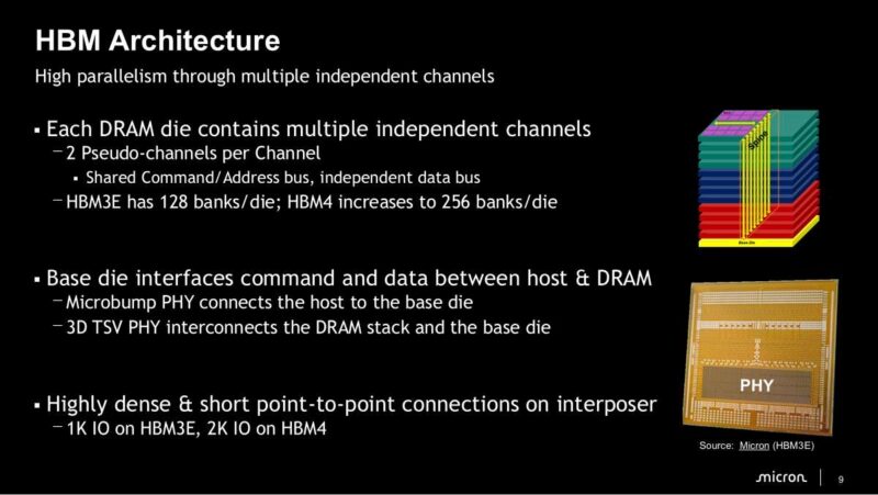
Each DRAM die holds multiple independent channels, with two pseudo-channels per channel, and HBM3E carries 128 banks per die while HBM4 doubles that to 256. A base die sits between the host and the DRAM stack, using a microbump PHY on the host side and a 3D TSV PHY into the stack, over highly dense point-to-point interposer connections that move from 1K IO on HBM3E to 2K IO on HBM4.
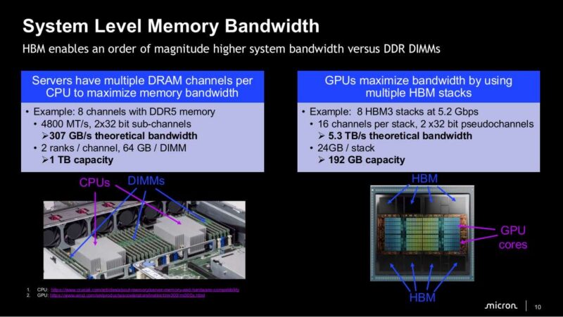
Micron is now showing the performance-versus-capacity trade-off. Something they are not really showing here is the difference in PCB area and power. Maybe that is for a future slide?
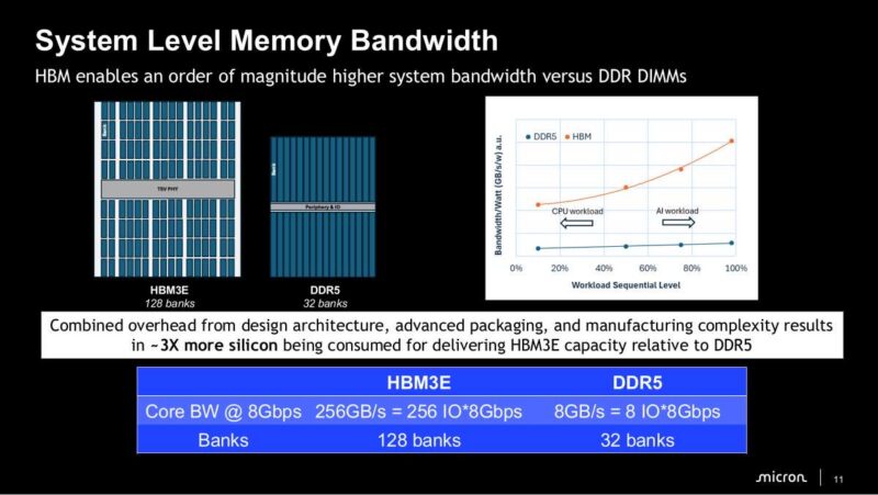
Micron is now noting the silicon cost of that speed. The combined overhead of design architecture, advanced packaging, and manufacturing complexity means that about 3x as much silicon is consumed to deliver the same HBM3E capacity as DDR5.
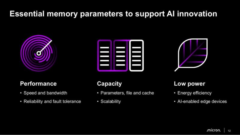
Micron’s presentation then summarized the memory parameters that support AI innovation in terms of performance, capacity, and power.
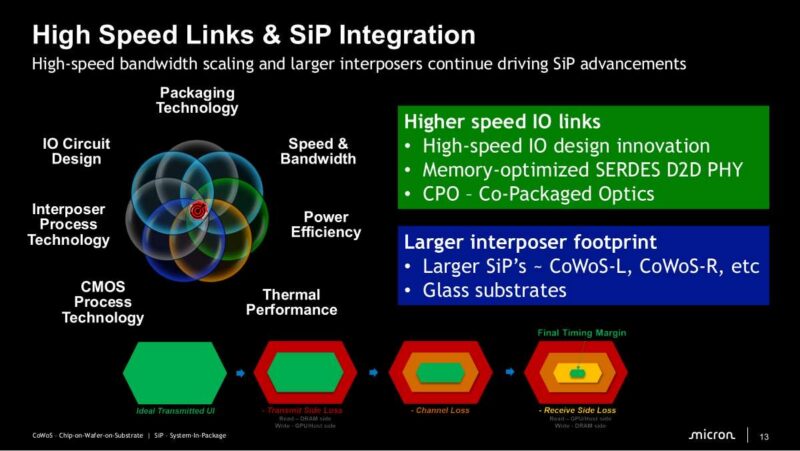
Higher speed IO links and larger interposers continue to drive SiP advances, with faster IO design, memory-optimized SERDES and die-to-die PHY, and co-packaged optics on the interconnect side. Larger SiPs along the lines of CoWoS-L and CoWoS-R and glass substrates are part of the packaging technology path.
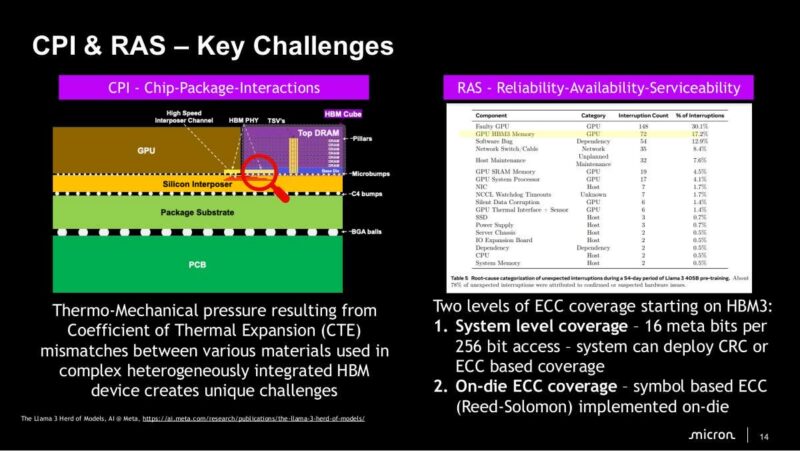
Now we are getting to reliability, including chip-package interactions and RAS challenges. Coefficient-of-thermal-expansion mismatches between different materials in a heterogeneously integrated HBM device create thermo-mechanical pressure. Actually, on a larger scale, that was one of the biggest challenges to make Cerebras’ WSE a reality. ECC coverage arrives in two layers, starting with HBM3, with 16 meta-bits per 256-bit access at the system level and symbol-based Reed-Solomon ECC implemented on-die.
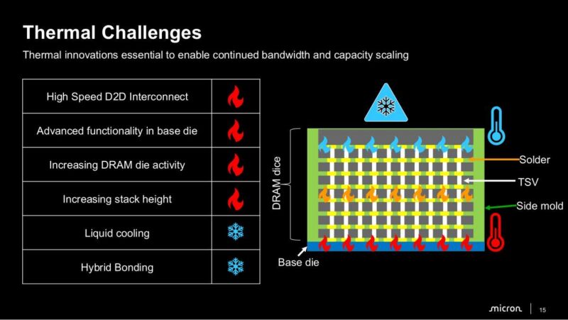
For thermal management, increasing DRAM die activity, higher stack heights, and more advanced base die functionality all add heat. Micron points to liquid cooling, hybrid bonding, and changes to the solder and side mold as part of the thermal innovations needed to keep bandwidth and capacity scaling.
It seems like we are nearing the end. With packaging trends.
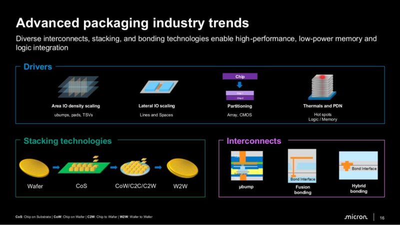
Taken together, these figures show how Micron is approaching evolving memory architectures for AI. Micron is balancing more HBM bandwidth and capacity against the packaging, thermal, and reliability costs of putting that much memory next to the compute.
Final Words
HBM is a big topic these days. Shifting capacity to HBM and the amount of it used by AI data centers are causing the current memory crunch. Micron is focusing on more than just capacity, and into packaging. These trade-offs among HBM bandwidth, silicon cost, thermal performance, and reliability will shape how accelerators are built over the next several generations. That is interesting since I expect we will see more on custom HBM with base dies that include memory controllers and compute this week.
We have a full recap on the Substack, including where all of these pieces ranked in terms of popularity: