Intel Xeon Max System Hands-on
The developer platform came in a ~115lb box, which is about twice that of an average 2U server. Part of the reason for this is it is designed not just for CPU Max development, but also GPU Max PCIe cards which were not populated in our system. One of the cool features of the system though was that the chassis was designed to stay in the rack while the portion with the CPU, memory, PCIe cards, motherboard, storage, and so forth could be removed. In higher-volume test environments like the Intel Developer Cloud, this makes servicing these systems much easier than standard 2U servers.
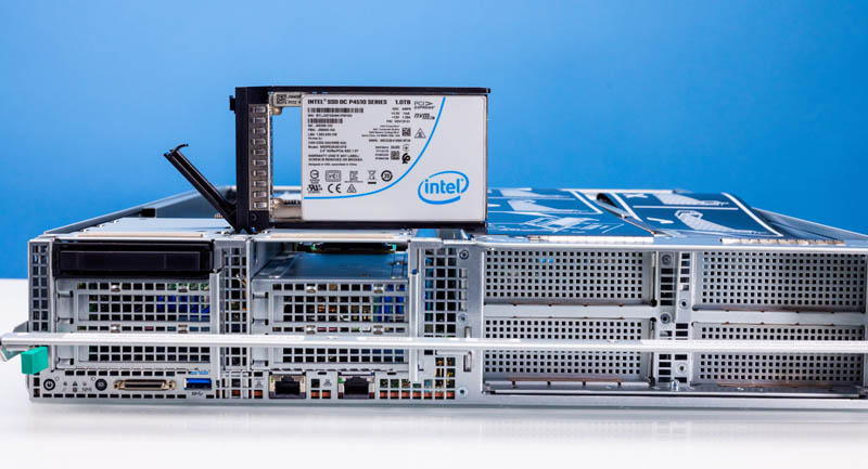
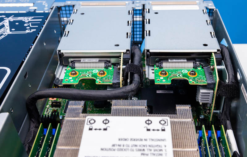
One fun design was the SSD backplane with vertical and horizontal PCBs for connectivity. After reviewing hundreds of servers, this is the first time I can recall seeing a design like this one.
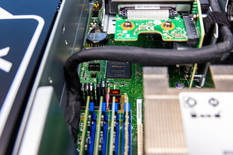
The CPU is not the only Intel “MAX” product found in the system, as there was an Altera FPGA, the MAX 10 onboard as well.
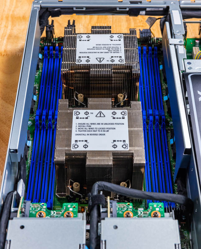
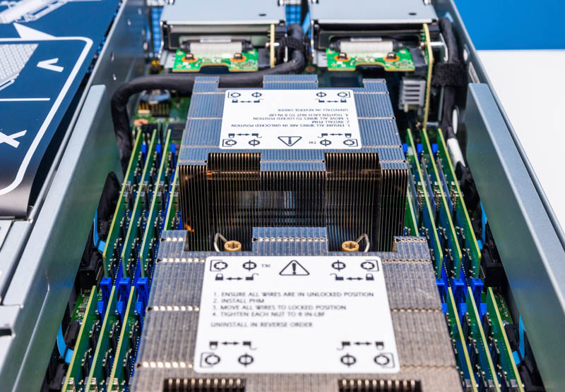
The CPUs themselves are 350W TDP units so we get large heatsinks. Notably, however, is that these are not liquid-cooled CPUs, they are still being air cooled.
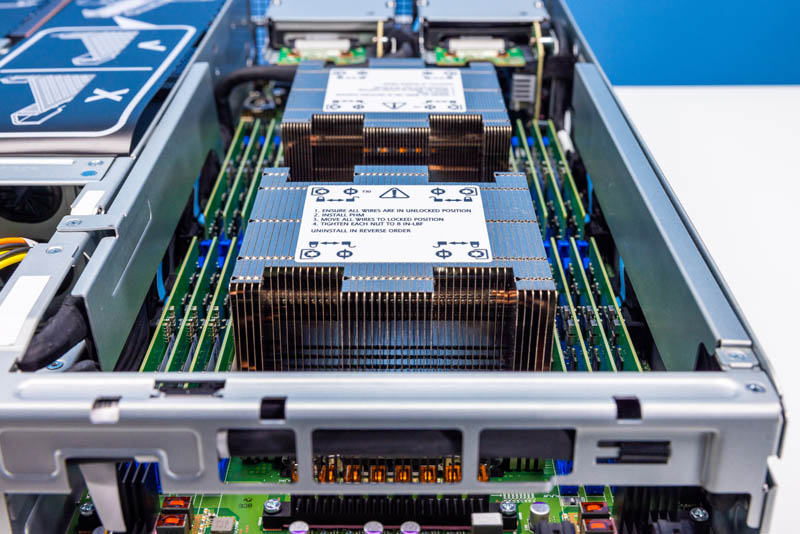
Here is another angle of the big heatsinks.
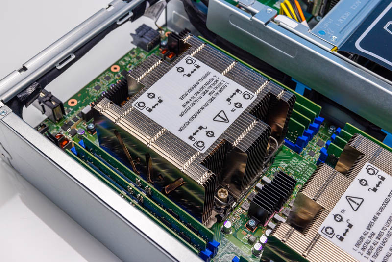
For our HBM2e-only testing, we took out the memory from the system. The default configuration had sixteen 16GB DDR5 ECC RDIMMs in the system, with eight per CPU. All of these DIMMs were removed for the HBM2e only testing.
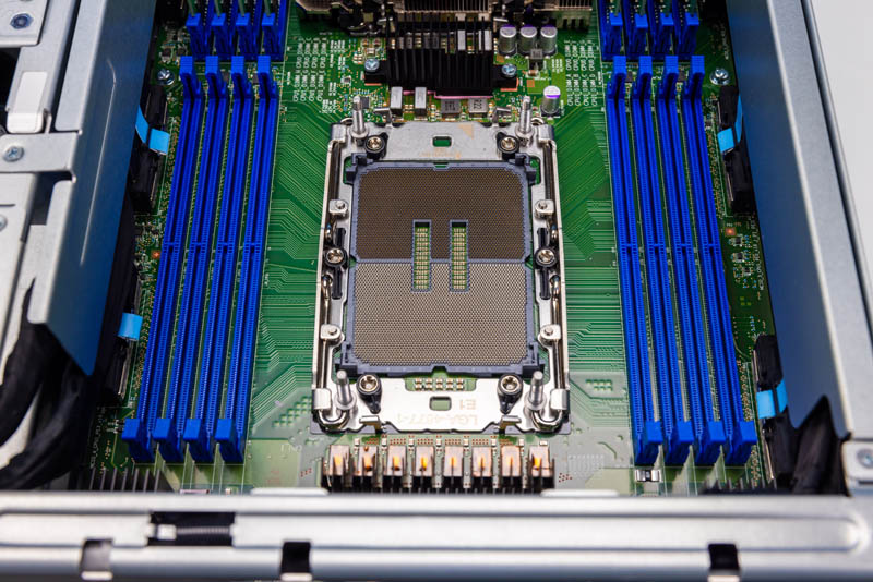
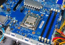
The CPU socket for the system looks like standard LGA4677 with one notable difference. The 8x DDR5 DIMM slots are a bit further than we are accustomed to seeing from the socket itself.
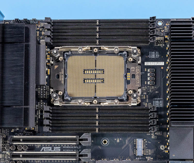
Perhaps not the best example, but here is a Xeon W-3400 series LGA4677 socket from our Building 3x Intel Xeon W-3400 Workstation and Servers with the ASUS Pro WS W790E SAGE SE where one can clearly see the minimal distance between the socket and the DDR5 DIMM slots on either side.
Our sense is that Intel did this for the development platform in order to fit wider heatsinks than we would normally see.
If a design goal is not having the narrowest CPU and memory area nor fitting sixteen DIMMs per CPU for 2DPC memory configurations, then this is a useful alteration to designs we normally see.
Next, let us get back to the Xeon Max 9480 chips so we can see how these memory slots are connected to the cores.


Terabyte per second STREAM is spectacular – this is comparable speed from a single server to running STREAM across an entire Altix 3700 with 512 Itanium processors in 2004, and rather faster than the NEC SX-7 which was the last cry of vector supercomputers.
Thanks for the power state info – I was wondering about 14 core/16GB HBM/dual memory consumer version. Oh well!
Despite what Intel stated by power states, I’d have at least tried booting the Xeon Max chip on a workstation board. Worth a try and it would open up a slew of workstation/desktop style benchmarks. While entirely inappropriate a chip of this caliber, I’m curious how a HBM2e only chip would run Starfield as it has some interesting scaling affected by memory bandwidth and latency. Be different to have that HBM2e comparison for the subject.
The open foam results don’t match between the two plots. Where one says hbm2e only is 1.85 times faster and the other says it’s only 1.05 times faster.
Can these be plugged into a normal workstation motherboard socket? as in a few years when these come on the market that mortels can buy off of ebay we wantto play with them in normal motherboards with normal cooling air cooling solutions
I had no idea that they’re able to run virtualization. I remember that I’d seen them at launch but I was under the impression that they’re only for HPC and that they’d done no virtualization and acceleration because of it. We’re not a big IT outfit, only buying around 1000/servers/year but we’re going to check this out. Even at our scale it could be useful
@Todd, Shhhhh! Quiet! Lest Intel hear you and fuse off the functionaility as they used to do…
Is that a real Proxmox VE pic? I didn’t think these could run virtual machines. Why didn’t Intel just call these an option if so. That 32c 64gb part sounds chill
It’s possible virtualization is not an advertised feature because there are too many information-leaking side channels.
At any rate, as demonstrated by the Fujitsu A64FX a couple years ago, placing HBM on the CPU package makes GPUs unnecessary and is easier to program. After the technology has been monetised at the high end, I expect on-package HBM will be cheaper than GPU acceleration as well.
Thank god there’s a good review of this tech that normal people can understand. This is the right level STH. I’m finally understanding this tech after years of hearing about it.
That STREAM benchmark result is impressive.
My 4GHz 16 core desktop computer copies value of double arrays at 58GB/sec, according to my STREAM build with MSVC, and I consider it as pretty decent, because it copies 15 bytes per 1 CPU clock cycle.
intel compiler should optimize STREAM for loop of double array copy with very efficient SIMD instructions