Intel had a cool technology on display at Hot Chips 2023, beyond just server chips. It had a direct mesh-to-mesh optical fabric. What might also be interesting is the 8-core processor with 66 threads per core.
Again, please excuse typos, these are being done live.
Intel Shows the First Direct Mesh-to-Mesh Optical Fabric
The key motivation behind this was the DARPA HIVE program for hyper-sparse data.
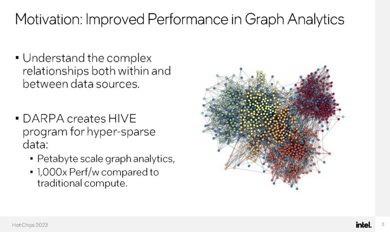
When Intel profiled the workloads that DARPA was looking at, they found they were massively parallel. Still, they had poor cache line utilization and things like big long out-of-order pipelines were not well utilized.
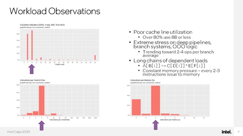
Here is an interesting one. Intel has a 66-thread-per-core processor with 8 cores in a socket (528 threads?) The cache apparently is not well used due to the workload. This is a RISC ISA not x86.
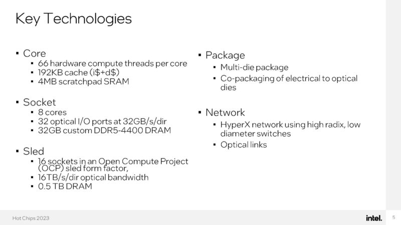
Intel is packing these into 16 sockets in a single OCP compute thread and using optical networking.
Here is the die architecture. Each core has multi-threaded pipelines.
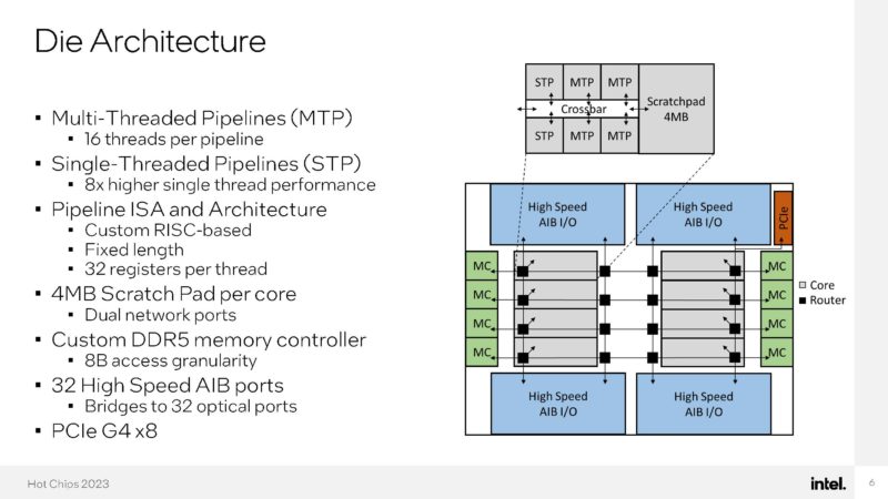
The high-speed I/O chips bridge the electrical to optical capabilities of the chip.
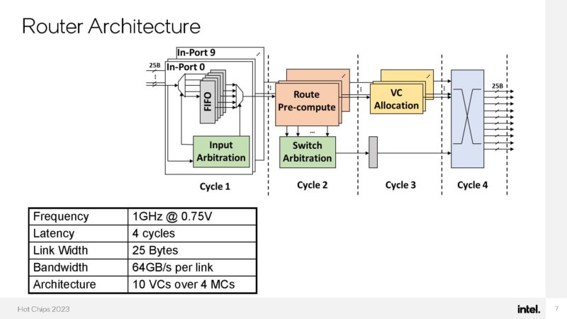
Here is the 10-port cut-through router being used.
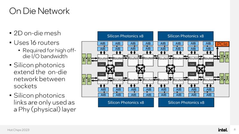
Here is the on-die network where the routers are placed. Half of the 16 routers are there just to provide more bandwidth to the high-speed I/O. On-packaged EMIBs are being used for the physical connection layer.
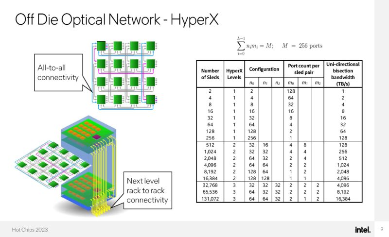
Going off-die, each chip uses silicon photonics to drive its optical networking. With this, the connections between cores can happen directly between chips even if they are not in the same chassis without adding switches and NICs.
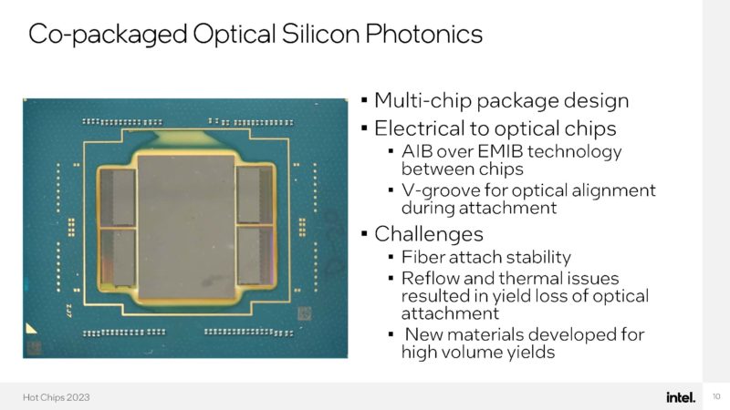
These chips are being packaged as a multi-chip package with EMIB. Having silicon photonics engines added a few other challenges of going from package to strands of fiber.
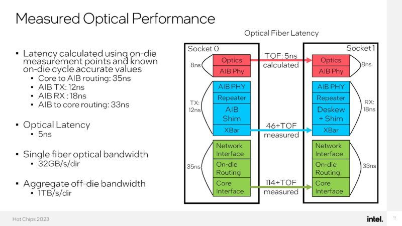
Here is the optical performance.
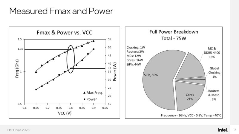
In terms of power, this was done in an 8-core 75W CPU. More than half of the power here is being used by silicon photonics.
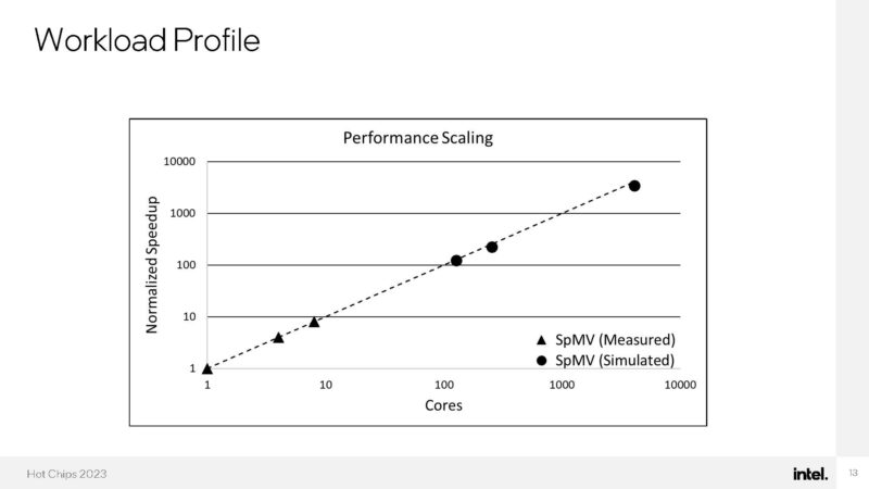
Here is the simulated to measured workload performance scaling.
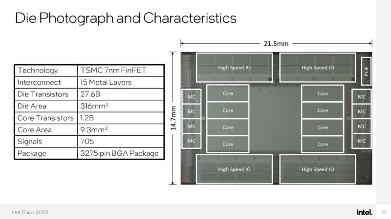
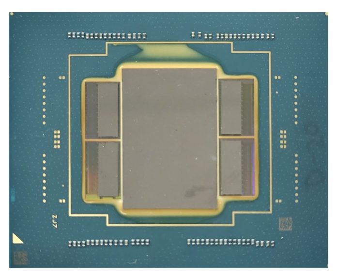
Here is the actual die photograph and confirmation that this is being done on TSMC 7nm.
Here is what the package and test board looks like:
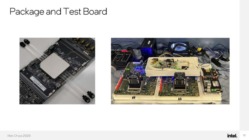
This was done in 7nm and work is still happening on this in the lab.
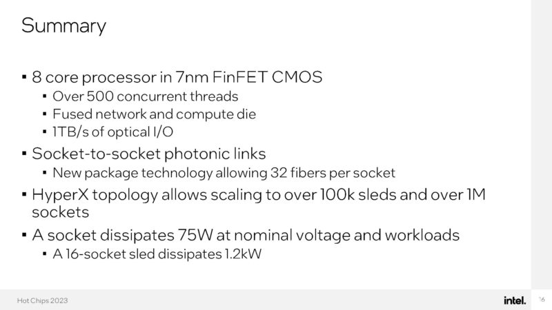
Final Words
It was interesting to see that Intel did not use the pluggable connector it showed off at Innovation 2022. It seems like this might have been built before that project was ready. This was assisted by Ayar Labs on the optical side.
Perhaps the big item is the 66 threads per core! That is a huge figure. I think folks will enjoy that stat.
Just as a heads-up, we are going to have a video later this week on the Intel Xeon Max (Sapphire Rapids with HBM2e onboard) and will even show it booting a hypervisor and running a VM all from HBM, without DDR5 installed. Intel has a lot of exotic chips either as projects or in production. Subscribe to our 250K+ YouTube channel to see all the fun things we get to do with chips like Xeon Max there.


Damn sakes. 66 threads? Per core? Is that a typo or have Intel really built such a thing? If that is, in fact, not a typo, that’s one damn big-ass processor (or maybe WIDE-ass since 8 cores is on the puny end but with 528 total threads, that makes it quite wide in terms of number of concurrent “channels/lanes” per core). Judging by the pics provided, the package, while big, doesn’t seem quite “mainframe-sized” enough to me for 528 threads to really be viable. Also, unless I missed it, there doesn’t appear to be any mention of what this RISC monster is being called. I’m assuming it isn’t ARM and i860 and i960 are both deader than a roast turkey on Thanksgiving Day. Very cool, though.
@Stephen Beets — I’m assuming this is some kind of funky research prototype.
Probably doesn’t get a marketing name any time soon.
https://dmccreary.medium.com/intels-incredible-piuma-graph-analytics-hardware-a2e9c3daf8d8 is from a few years ago about this HW.
Perhaps some fruits from the Risc-V good will Intel has been spending out?
Nice little micro services box. Mainframe like really.
how about performance per watt of this photonic CPU ?
From my understanding, this is purpose built processor to perform large graph traversal.
On graph traversal tasks, each thread just load then conditional store and ALU or other singleton resource of the processor is rarely used
and efficiency is scaled well by increasing just execution unit.
I remember similar purpose built CPU, Sun Niagara processor which is designed solery for web server tasks, and one floating point unit is shared by 8 cores (32 hyperthreads)
@Stephen Beets, since the threads for the target workload issue a memory load every few commands, which takes on the order of 100 clock cycles to complete, they spend the vast majority of the time idle. having 66 threads per core allows those memory loads to execute in parallel. as the data for different threads arrives on the order of every clock cycle, commands are dispatched to the execution units nearly every cycle, so the execution units achieve a high overall utilization.
@antonio Wow, thanks for the interesting article you linked to. Lots of deep technical stuff in there that goes way over my head, so unfortunately I skimmed through most of it but the gist I got is that this chip here is part of the DARPA HIVE project and this little beastie is for “graph analysis”. Apparently that’s important for AI. Very fascinating. I guess I should have suspected this was some AI thing.
@J Thanks for your breakdown of what the huge thread count per thread is for. I did not know that memory loads take up so many clock cycles. You don’t really notice that on a normal (heh heh “normal”) PC when running regular programs. I guess “graph analysis” is so specific that it needs separate hardware and not any old CISC CPU or GPU can cut it.
I guess this comment can be summarized as “What is a core anyway”, but from looking at the slides (slide 6 specifically), I wonder if its really accurate to describe it as 8 cores and not 8 core-clusters.
With 6 separate pipelines, what resources does a “core” share that makes it a single core?
I don’t think some shared scratchpad and interconnects reaches that threshold.
Obviously intel knows more about this architecture than me and they call it a core, but it sounds strange to me.