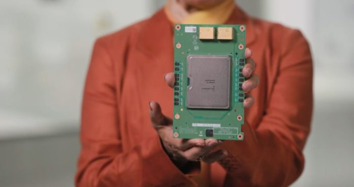
At Intel Architecture Day 2021, Intel disclosed more about its new HPC-focused GPU offering: Ponte Vecchio. If there was any question of Intel’s desire to embrace multi-die/ multi-tile and multi-fab, this is the product that will put those questions to rest. The Intel Ponte Vecchio Xe HPC GPU is a Spaceship of a GPU. Whereas we previously called those working on making chips chip designers, if Ponte Vecchio is a “spaceship” that would make those working on it “chipbuilders.”
Intel Ponte Vecchio is a Spaceship of a GPU
Intel is targeting more than a small departure with its Xe HPC GPU codenamed Ponte Vecchio. A few years ago the company recognized that Xeon Phi was not going to get the company to exascale fast enough. Instead, it needed a GPU architecture with a radically different approach. Here is the improvement that the company is targeting:
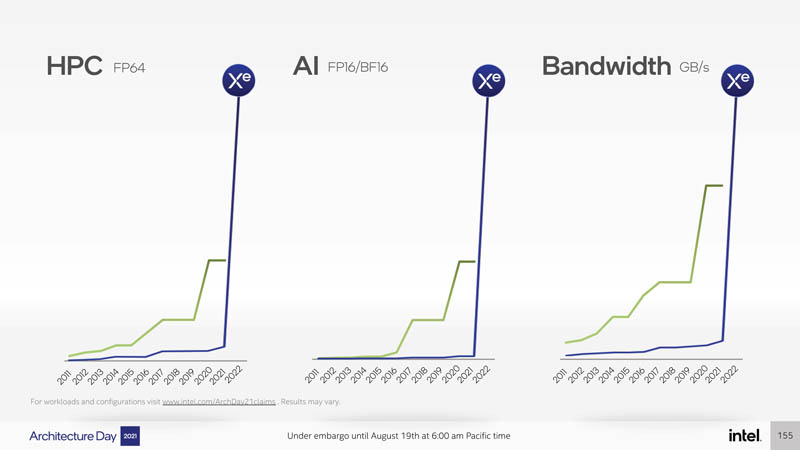
The green line is NVIDIA’s top-end GPUs like the NVIDIA A100’s we looked at in Liquid Cooling Next-Gen Servers Getting Hands-on with 3 Options and Inspur NF5488A5 8x NVIDIA A100 HGX Platform Review. The blue line does not have a scale, but Intel’s point is that it is expecting big gains.
Intel Xe HPC Architecture
The Intel Xe HPC architecture incorporates a number of different IP tiles, but perhaps the main one is based around the Xe-core. This is the compute unit of the Xe HPC GPU. There are 8x 512-bit vector engines and 8x 4096-bit matrix engines. These execution units get a sizable L1 cache and the ability to move data quickly in order to keep them fed.
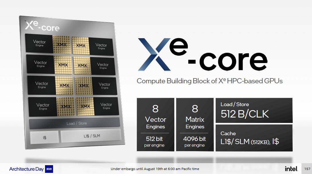
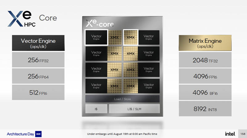
Here are the specs for the Vector Engine and Matrix Engine.
The building block of the Xe HPC core is then assembled into the Xe HPC Slice that aggregates 16 of these cores together. Since each has 512KB of L1 cache, that gives us 8MB of L1 cache total. A key challenge in GPU designs is memory bandwidth, or put more simply, keeping execution units primed with data to perform useful work. Much of the Xe HPC architecture is designed to keep the execution units primed as much as possible.
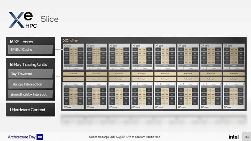
In the middle of the Xe HPC Slice are the 16 Ray Tracing units. Also as a quick note, the hardware context here is designed to help accelerate things like virtualized/ multi-tenant GPU usage.
Up to four Xe HPC Slices are brought together with a large L2 cache, 4x HBM2e memory controllers, a media engine, along with the Xe Links to form the Xe HPC Slice. In the bottom corner, one will notice the “Stack-to-Stack” block.
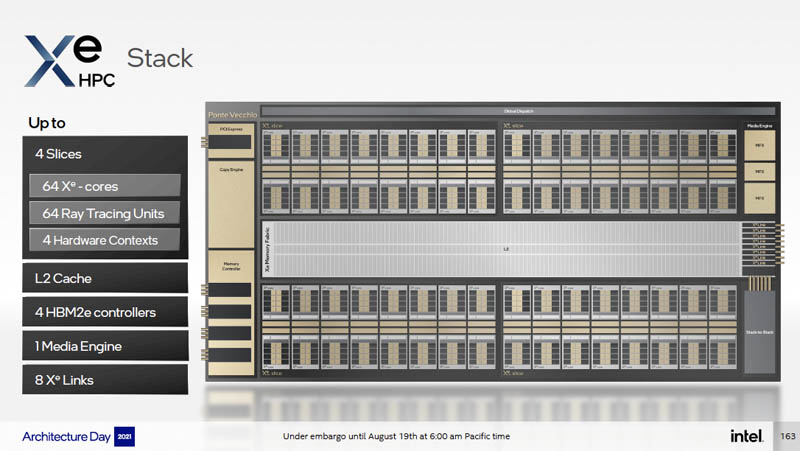
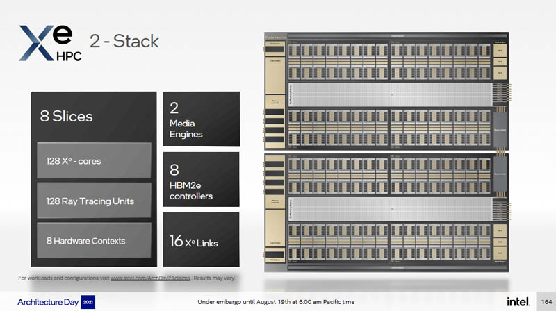
That is for the Xe HPC 2-Stack that combines two of these stacks for a total of 128x Xe HPC cores/ 8x slices together. As a result, we get eight times the slice figures for things such as 128x ray tracing units as well. We also double features such as the Xe Links (16) and HBM2e memory controllers (8.)
The Xe Link is the high-speed coherent unified fabric that allows for GPU to GPU transfer. We are not going to say this is Intel’s answer to NVLink, but a reader can draw their own conclusion.
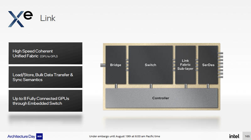
The Xe Link can be used to connect two, four, six, or eight GPUs together.

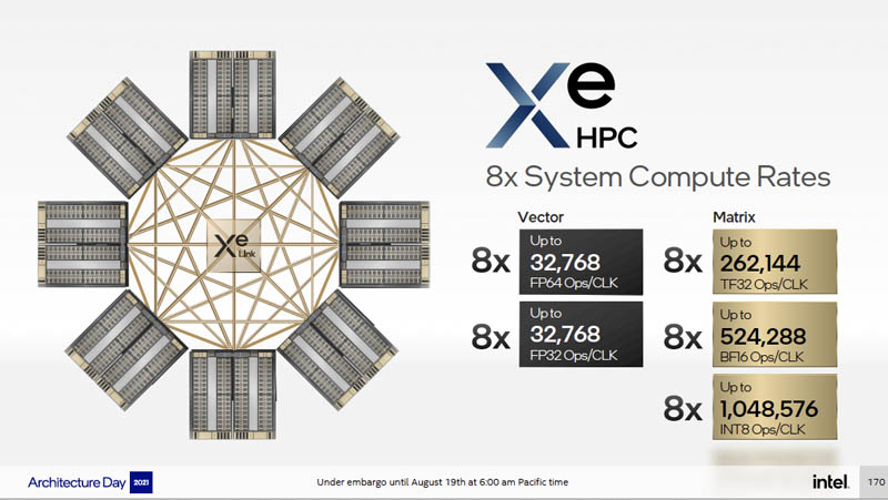
If one has eight Xe HPC GPUs in their full configurations (there are many “up to’s” in the slides), here are the performance figures:
Now that we have looked at the architecture, let us get to the Intel Ponte Vecchio Chipbuilding.



Quanta costa… I guess not cheap GPUs these Ponte Vecchio
“The Xe Link is the high-speed coherent unified fabric …”
Previous presentations on Ponte Vecchio mentioned CXL, and I presumed the Sapphire Rapids chips would be responsible for coherency. I didn’t hear CXL mentioned for Ponte Vecchio today, nor for any of the other chips except Sapphire Rapids.
It seems there are late on cache coherency compared to AMD which handle it between EPYC and Instinct MI200
“Like a spaceship that hurdles mankind”…
Surely you mean hurls?
Can it run Crysis, tho?
Intel bought up most of tscm 3 nm production lul who cares what amd does