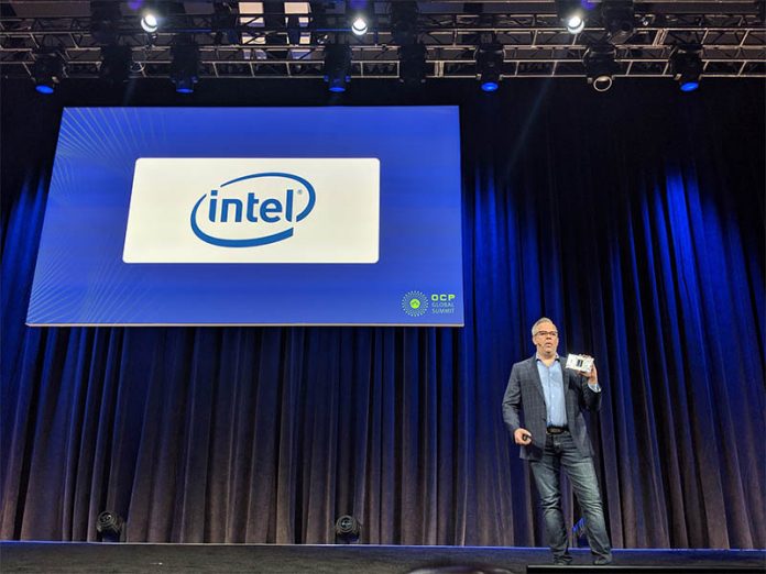
Jason Waxman gave the Intel OCP Summit 2019 keynote as he has done in previous generations. During the keynote, Intel focused on some of their upcoming hardware roadmaps across a number of areas. Here are a few of our highlights from the keynote.
Cascade Lake and Cooper Lake with DCPMM
Intel showed off both Cascade Lake which we expect soon, as well as Cooper Lake which is expected in a few quarters.
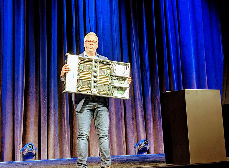
Intel’s discussion focused on not just traditional two socket designs but also scaling up to four-socket and eight-socket designs. In a four-socket server, Intel said it can hit 112 cores and 224 threads. Also, Jason said that the four-socket Cascade Lake server will hit 12TB of Intel DCPMM. You can see our teardown of Intel DCPMM modules in A Close Look at Intel Optane DC Persistent Memory Modules and Intel Optane Persistent Memory Looking at Green Apache Pass DIMMs or on YouTube:
Intel showed off Cooper Lake in 2S, 4S, and 8S configurations. The Cooper Lake platforms were built in dual socket blocks so that the 4S is denoted as 2x 2S while the 8S platform is denoted as 4x 2S.
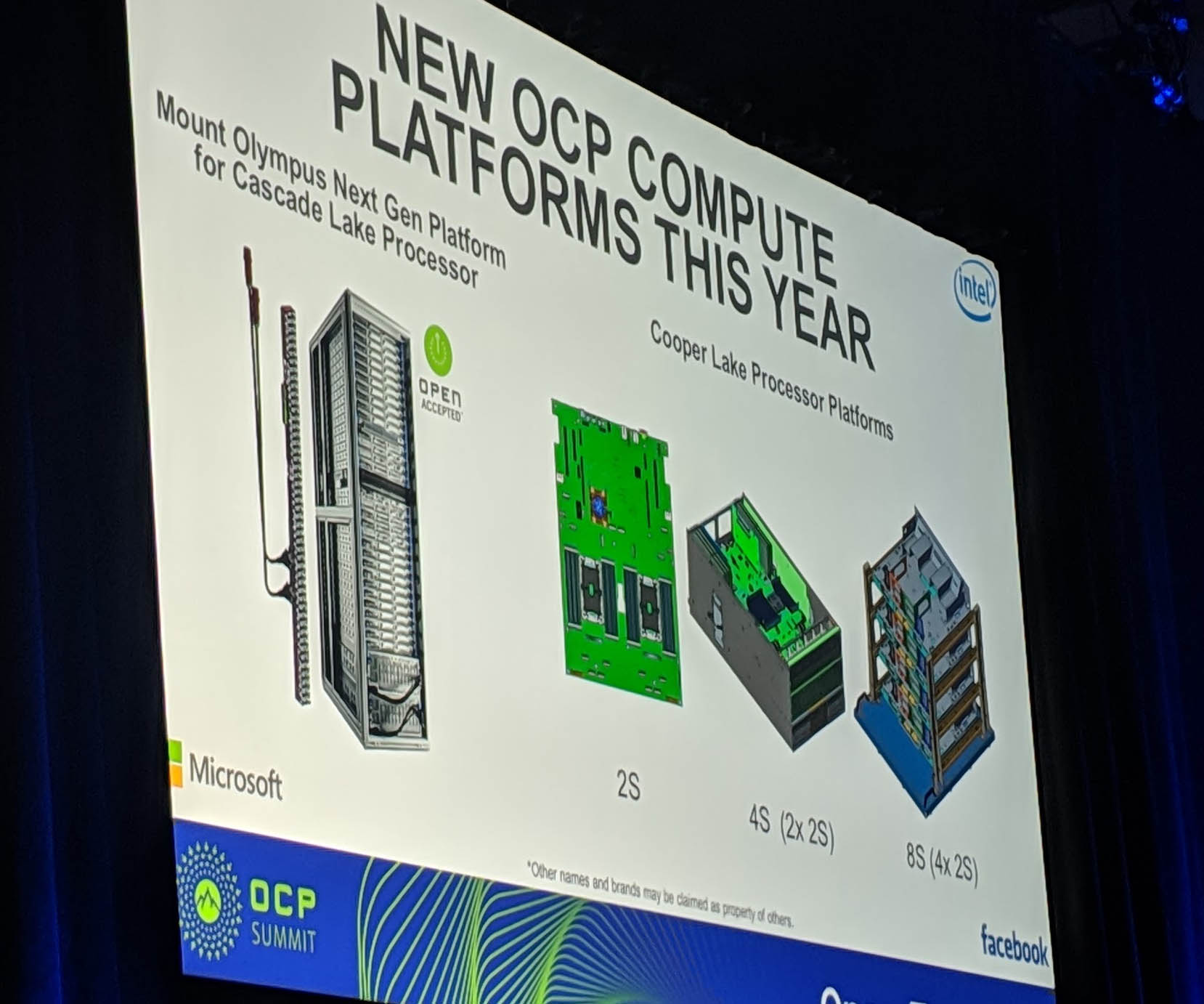
Somewhat tellingly, there was no mention of Cascade Lake-AP at the OCP Summit as we expect that to be a niche platform.
New AI and Deep Learning Chips
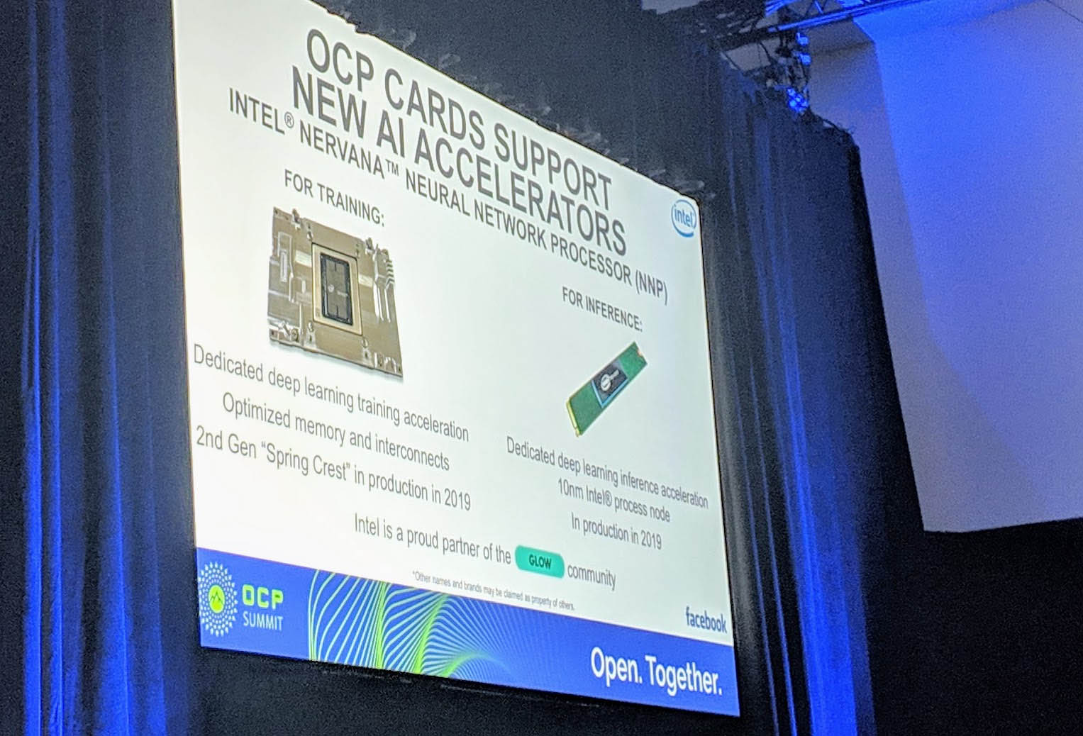
Intel said its second-generation “Spring Crest” Nervana NNP will be in production in 2019. The first generation was largely a development project that found its way to Facebook (an OCP founding member.) We are hoping the second generation sees more widespread deployment as this is a space that needs more competition.
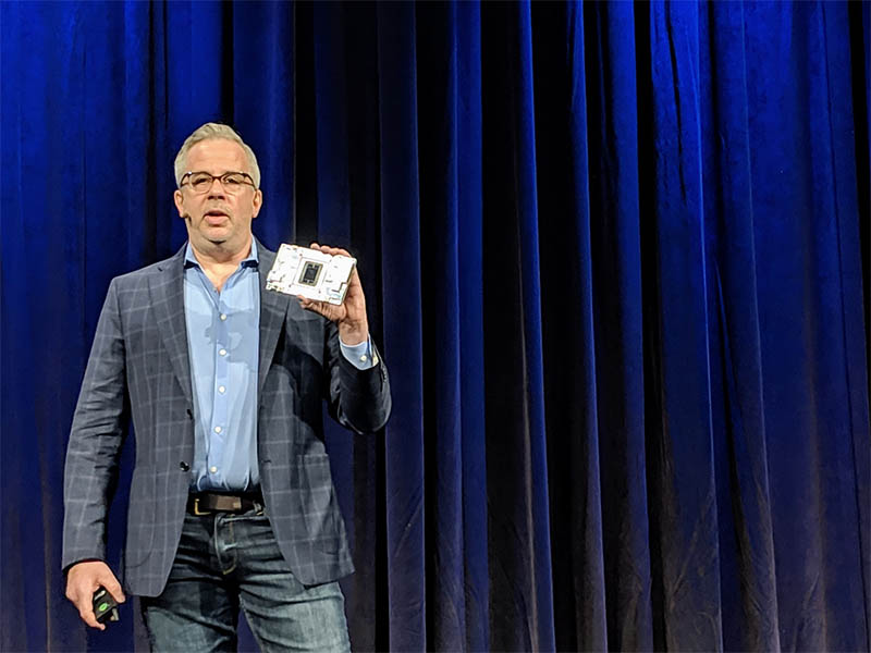
Intel also addressed inferencing using a 10nm M.2 module that will be in production in 2019 as well.
More on Intel CXL
Intel CXL is expected to be available in the future using PCIe Gen5 x16 physical and electrical connections at 32 GT/s. You can read more about the announcement in our piece earlier this week in: Intel CXL Compute Express Link Interconnect Announced.
Networking and Silicon Photonics
New OCP Gen3 100GbE NICs in the second half of this year. Intel also said that it is looking at how it can use silicon photonics to help enable lower power consumption in the 400GbE generation.
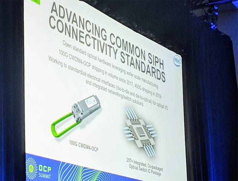
I apologize for the slide offsets. I am sitting in the middle of the stage and slides are being projected far to the side, not on the center screen.



Whateverlake, still with “Spoiler” inside or not?
U.S. banned Huawei and has been having its allies do the same for security reasons (proven or not?), but does U.S. have the balls to do the same to Intel for the PROVEN security problem of “Spoiler” (caused by its INTENDED design) with no effective patch?