Intel went into more detail on its upcoming hybrid SoC. Intel Lakefield is a SoC that combines different pieces silicon using Intel 3D Foveros packaging. In the process, Intel validates the AMD EPYC 7002 series and Ryzen 3000 series strategy is the way forward. At the end of the day, this is a big step forward and is a shot across Qualcomm’s bow as well as a technology demonstration of what Intel is capable of. 3D Foveros is a higher-end process technology versus what AMD is using at this point on CPUs.
The Intel Lakefield Hybrid SoC
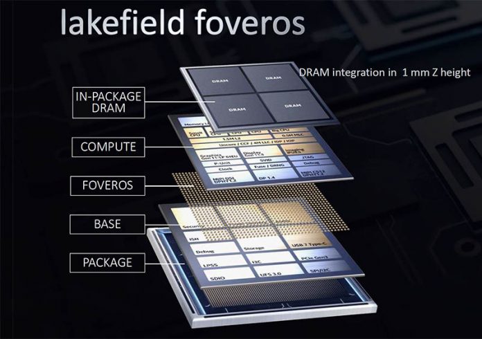
The 10nm compute die has the Sunny Cove core plus four Intel Atom cores along with the GPU functionality. This is a big deal. Intel now has a big hybrid core. The lower die is all of the I/O. Intel is calling this the base die on P1222 process. If it sounds familiar, AMD has moved its desktop and server CPUs to an I/O Die.
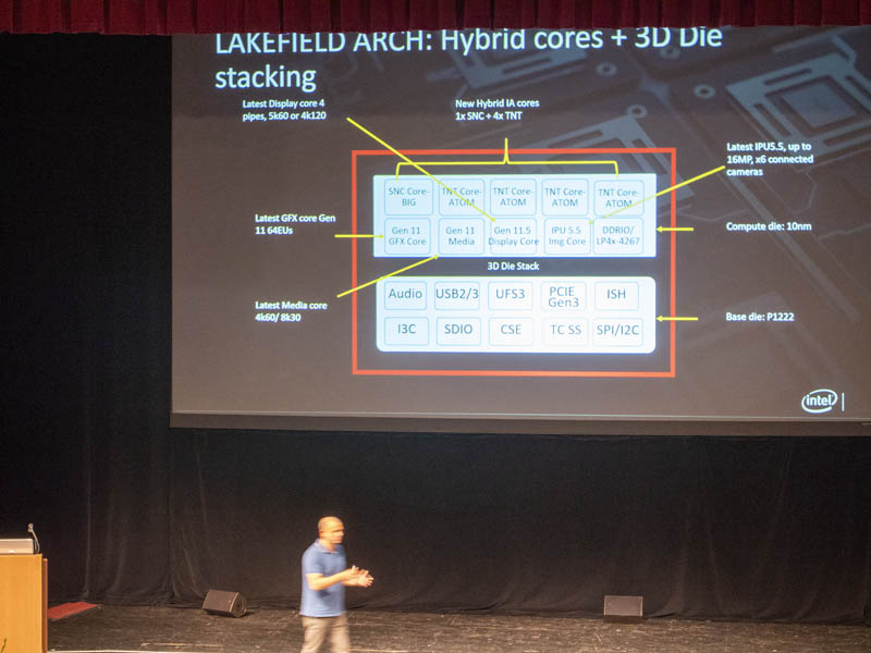
On stage, Intel said you cannot satisfy all needs for performance and power in a single die. One monolithic dis is what Intel uses in the current 2nd Generation Intel Xeon series.
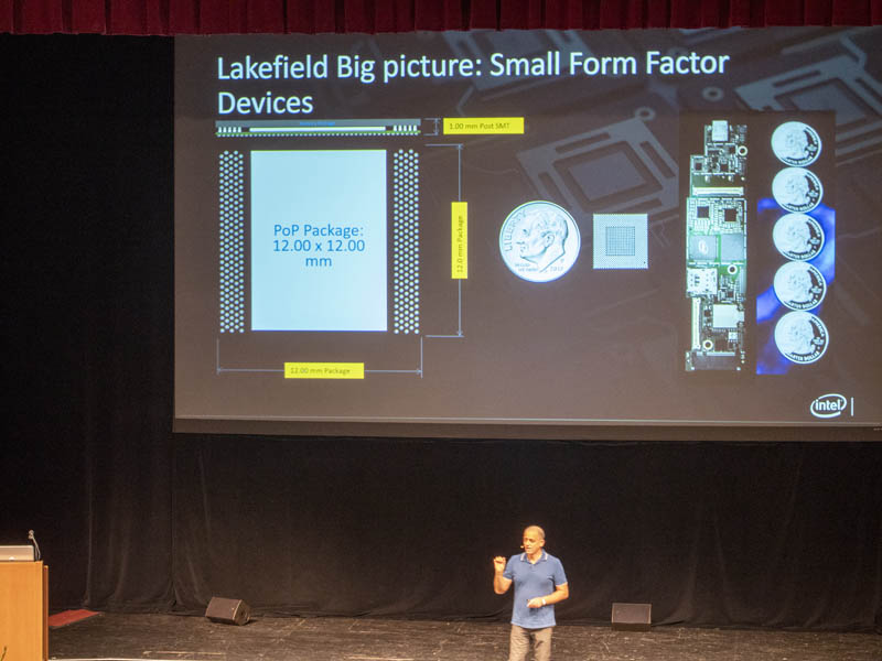
Intel also has a POP memory configuration. Here, Intel integrates memory into the package as well. The base configuration puts 4GB of RAM, the Sunny Cove big CPU core, four lower-power Atom Tremont cores, GPUs, and I/O all into a 12x12x1mm package.
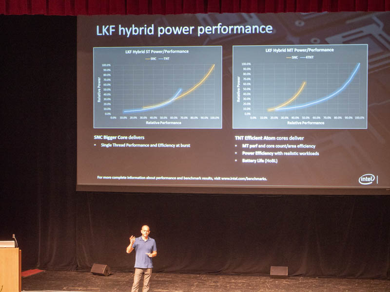
The benefit of combining both types of cores is that one can get higher single-threaded performance with Sunny Cove and get lower power and better multi-threaded performance with Tremont cores.
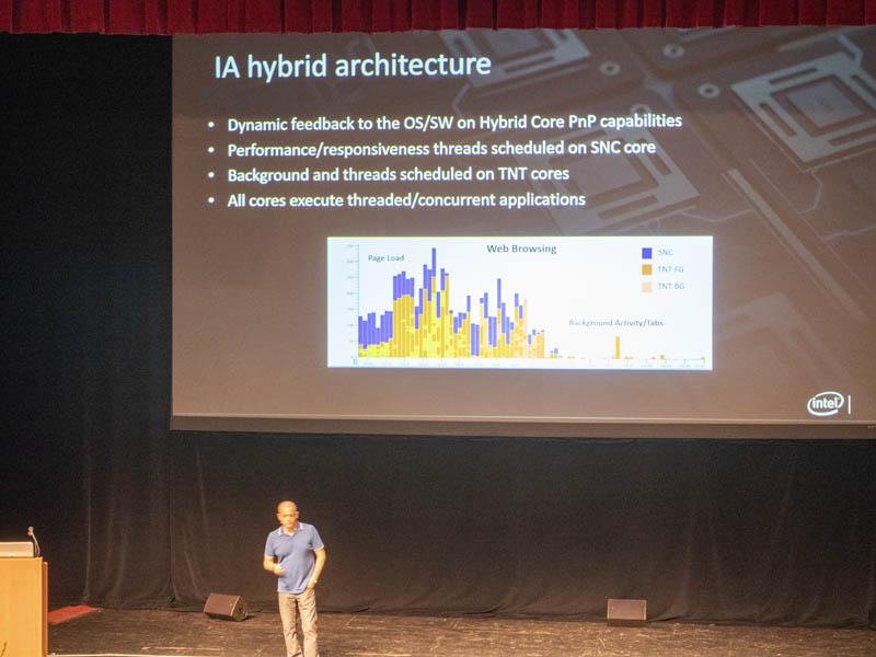
Intel is able to give feedback to the OS about the hybrid core capabilities. In that way, it can schedule on the Sunny Cove cores for performance and on the Tremont cores for lower power.
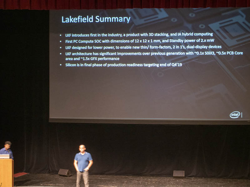
With the stacking, an Intel Lakefield SoC uses less than 1/10th of the standby power as standard Intel Core parts.
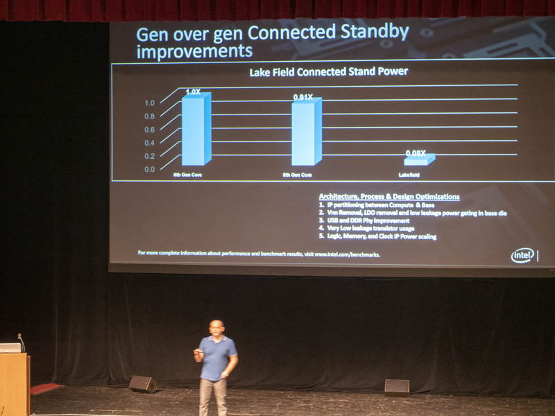
Lakefield has a lot of firsts. It uses 3D stacking and Intel Architecture hybrid computing. It is the first PC SoC that fits everything in 12x12x1mm and standby power.
Final Words
Intel Lakefield is in the final phases of getting ready for production. Production samples will be ready for late Q4. In late 2018, we thought we may see these chips this year. Now is looking like consumers may not see these chips until 2020. We still want to see Intel Xeon D Hewitt Lake and Snow Ridge SoCs.


Rome must be really very good: Intel is just spamming out the product announcements this past couple of weeks.
Does this also allow AVX-512? And if so, how?
Patrick….these are not SoCs (system on a chip) In fact these are the antithesis of SoC. 3D stacking with chiplets is “dis- integration” so that functions can be manufactured in the best technology and node possible and recombined. Anything 3D is by definition NOT SoC. Don’t mean to be a hardass about nomenclature but……..
I agree with Phil. These look more like Package On Package (POP) designs. Depending on where the connections lie, one could even consider them 3D System in Package (SiP). But the point being, they’re definitely different components stacked with interconnects added.
P1222 is the process used for the lower die, not the die’s name.