

For our second presentation from this morning’s first CPU session, we have Intel, who is presenting on their Core Series 3 chips. Also known by the codename Wildcat Lake, Intel launched this family of chips earlier this year as the budget counterpart to Core Ultra Series 3 (Panther Lake). This morning’s presentation, in turn, goes into the architecture of Wildcat Lake, while discussing some of the engineering tradeoffs Intel made to hit their BoM and power targets for their first high volume and low-priced chiplet-based CPU.
Please note, we are covering this live, so please excuse typos.
Intel Core Series 3 (Wildcat Lake) CPU at Hot Chips 2026
As the first of Intel’s triad of presentations of Hot Chips, the Wildcat Lake talk is a look at Intel’s low-power and low-priced SoC for budget and edge devices. While the bulk of these chips will end up going into consumer devices, Intel also as a decent edge device market where these chips are being deployed as well. And to that end, this is part of Intel’s toolset for covering a full spectrum of markets, from the edge all the way to data centers and servers (Diamond Rapids).
Wildcat Lake is notable here in that while it is a distinct silicon design from Panther Lake, it is (largely) not a distinct architecture. Intel has reused their Panther Cove and Darkmont CPU cores here, as well as the Xe3 GPU architecture. Though everything has been scaled down to make a smaller and cheaper chip
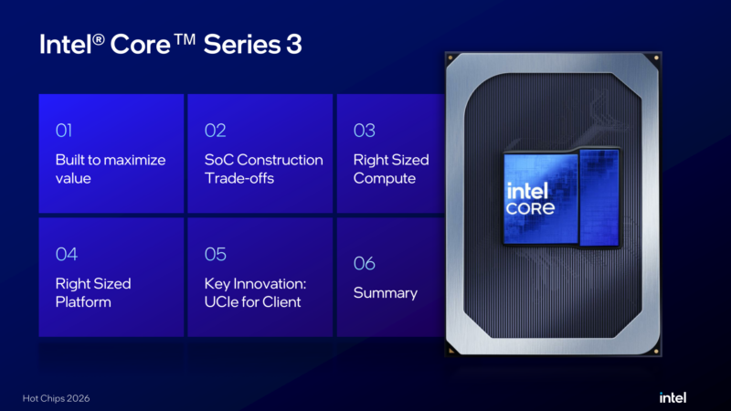
Here’s a high-level look at what Intel will be talking about with this presentation. Among the highlights: the construction trade-offs, what and how Intel deemed the chip to have the right amount of execution units and features, and how they used UCIe to cheaply connect the chiplets – a first for Intel.
“Why are we excited to share this product with you today?” Intel wants to give the audience a look at the behind-the-scenes decisions and why it came out the way it did. It came down to maximizing the value for the entry-level segment.
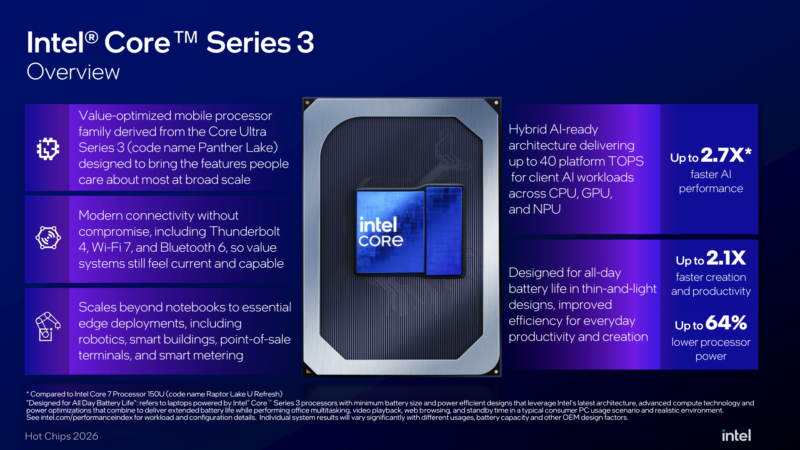
Core Series 3 is derived from Core Ultra Series 3. Much of the time the way to a budget chip is to do a gen -1 (or -2) design. But for this generation, Intel wanted to deliver their latest and greatest architecture to the budget market. This also garnered the Wildcat Lake team Intel’s latest platform technologies such as Thunderbolt 4, the Xe3 GPU architecture, and Wi-Fi 7.
Intel’s last generation product in this line was Raptor Lake-U, an Intel 7 process product. So they have skipped a generation of process nodes here, going from 7 to 18A.
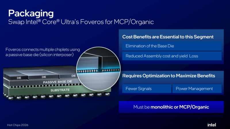
Packaging was apparently a hard decision for Intel. Foveros gives Intel a lot of capabilities and flexibility, as it allows for very small and well-connected chiplets/tiles. Not to mention it’s easier for validation. However Intel doesn’t need that kind of flexibility for a budget chip, and the dies are smaller to begin with here versus Panther Lake. MCP/organic packaging is the only way for Intel to hit their affordability targets while using a chiplet design. UCIe, in turn, was the key technology that enabled Intel to use MCP here rather than Foveros for their chiplet interconnect.
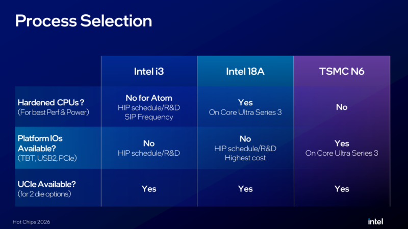
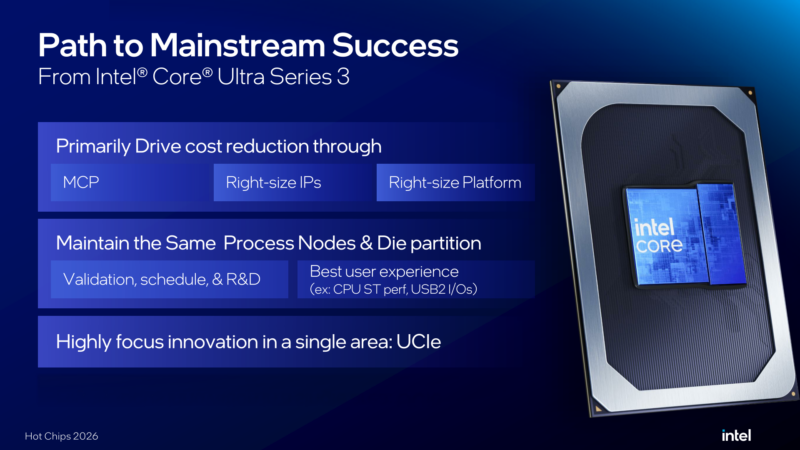
These decisions allowed Intel to focus their development and innovation on right-sizing the IP and utilizing UCIe to connect the chiplets.
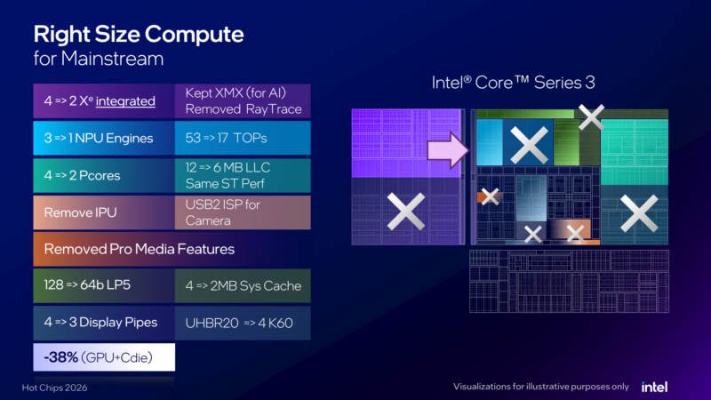
Here’s a look at how Intel cut-down Panther Lake for Wildcat lake. Fewer P cores, fewer NPU engines, a smaller GPU as well. Intel dropped ray tracing here, but they did keep the XMX cores (though they wanted to drop it initially). They also removed quite a bit of cache, and downsized the display controller by removing things like DisplayPort UHBR capabilities.
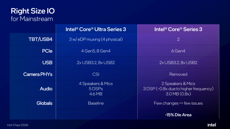
As for IO, Intel kept Thunderbolt 4/USB4 connectivity, though with just 2 heads. The rest of the USB system was kept largely identical. There are fewer PCIe lanes, however, and the camera PHYs were removed entirely. Other parts, which Intel terms the “globals” were left unchanged because they involve a lot of validation, which Intel wanted to avoid duplicating/redoing unless necessary. Altogether this saved Intel about 15% in die area for the I/O chiplet versus Panther Lake.
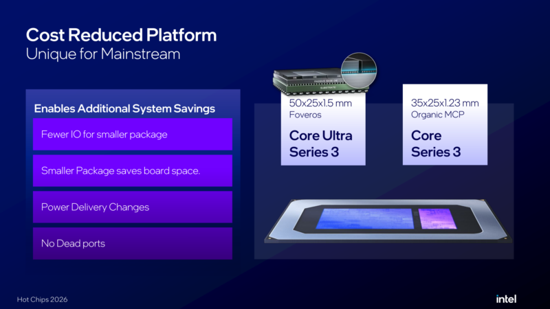
Wildcat Lake’s package is also quite a bit smaller than Panther’s. Not to mention much cheaper being organic multi-chip instead of Foveros.
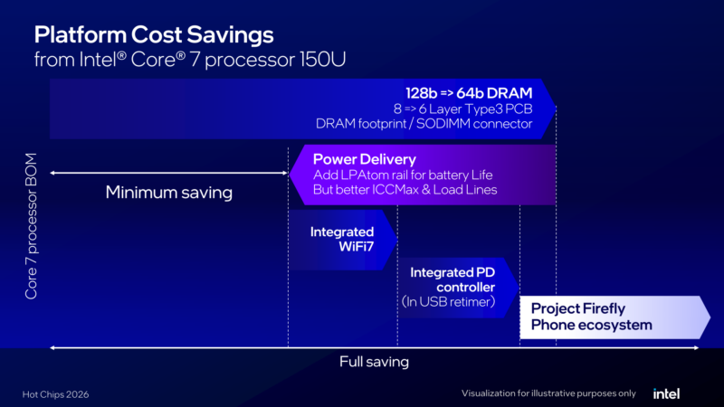
Intel opted to go with a narrower DRAM bus for Wildcat, which cuts down on the cost for system vendors. Whereas in other areas they kept things unchanged, such as the dedicated power rails for the E-cores and the GPU, which is a big part in driving the energy efficiency of Panther and Wildcat Lakes. The high level of integration of features such as Wi-Fi 7 was also a big gain that Intel kept here, as it keeps the cost of systems down for vendors.
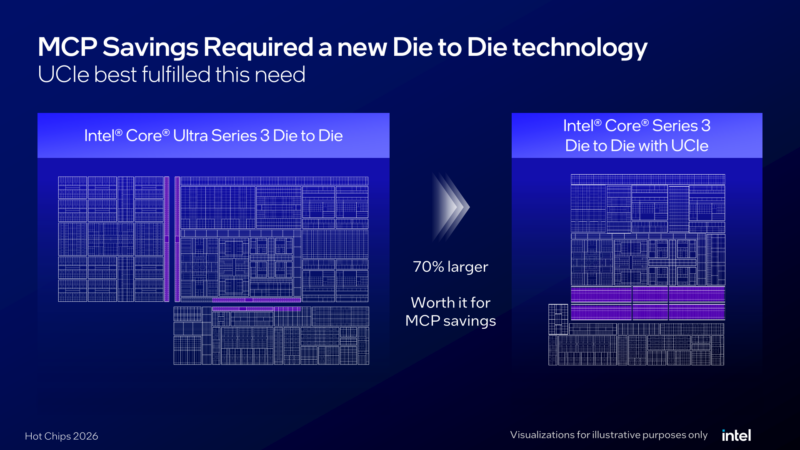
For Wildcat Lake, Intel went down to just 2 dies. And rather than using complex Foveros, they went with cheaper organic packaging, with UCIe providing the actual die-to-die connectivity. Intel did look at doing a monolithic die as well and forgoing chiplets entirely, but with IP availability and the actual costs of chiplet fabbing and assembly favored the 2 die MCP format.
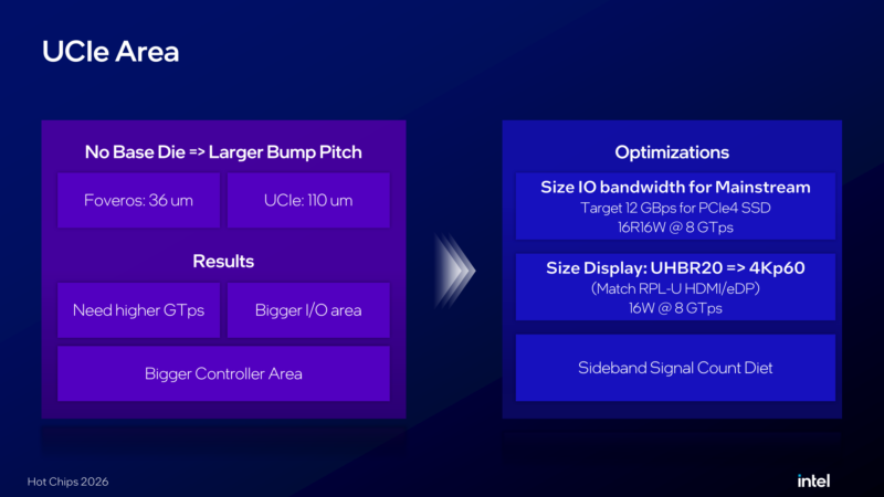
Advanced packaging has a pitch of about 36 microns, organic UCIe is around 110 micron. The lower density D2D connection keeps the costs down, while also reflecting the smaller amounts of data the chip is throwing around. There’s less I/O bandwidth from fewer PCIe lanes, there is less display bandwidth needed because the display controllers do not support the same high bitrates modes and resolutions.
The validation team also got a shout-out at Hot Chips. A lot of effort went into making all of this work.
UCIe also meant that Intel had to learn how to efficiently packetize their D2D communications. Foveros is not packetized, whereas UCIe is.
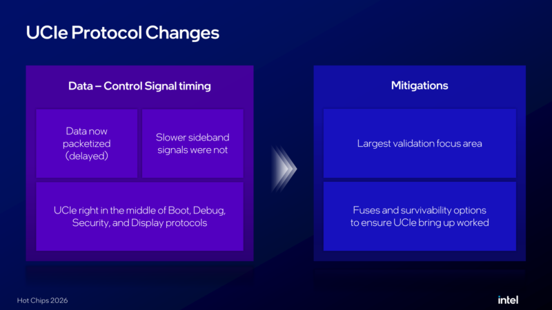
Intel implemented buffers where possible. Be it a register or some other kind of fuse to help ensure that the UCie bring-up worked.
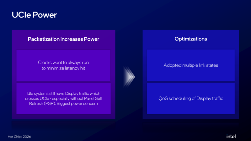
Power was another big concern for Intel for using UCIe. They have to run display traffic across the dies almost constantly, in part because cheap laptops often don’t have panel self refresh, where the displays are more independent. This was critical for meeting Intel’s battery life targets. To do this, they buffered the display links between dies in order to let them go to a low power state and then burst the data once the buffers were full.
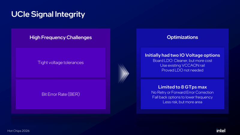
And, of course, there is always the matter of signal integrity. Intel’s power analysis team did a lot of work here. Intel opted to put a second LDO on the board as a backup plan in their design. It ended up not being needed, and it could be removed later.
Meanwhile, keeping the links limited to an 8 GT/sec rate kept the bit error rate low. It meant they could avoid needed retry and forward error correction techniques. It ate up more die space by requiring a larger number of lanes, but it kept the complexity down, which was the bigger risk.
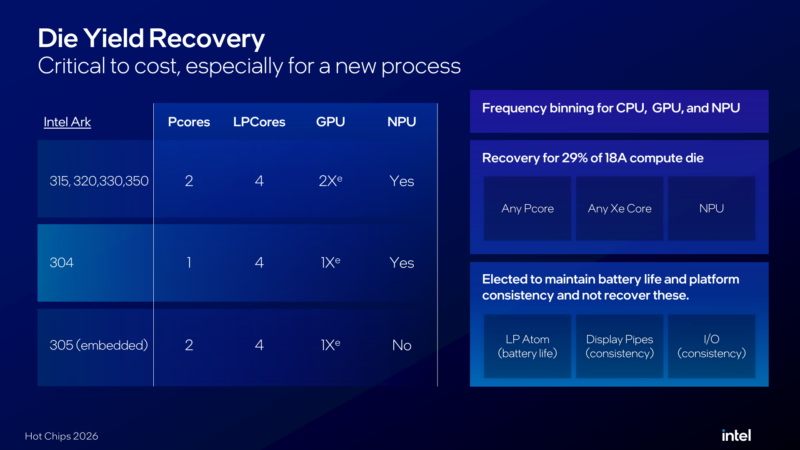
And here is a look at die yield recovery. Intel has multiple configs to use recovered chips, and about 29% of compute dies were recoverable with their current chip SKUs. The balancing act is that SKUs that customers do not want (or are not useful) is not helpful to recovery in practice.
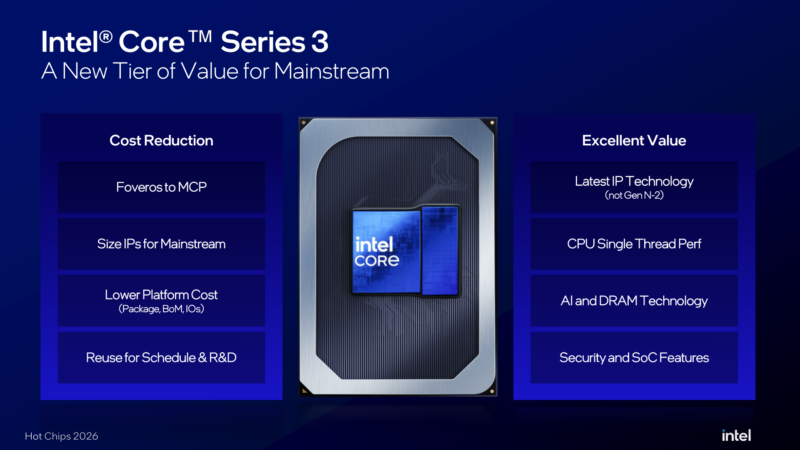
Overall, Intel’s Wildcat Lake team is very proud of what they accomplished with the chip. They hit the cost targets, they hit their performance targets, they were able to integrate UCIe connectivity as a first for the company. Consequently, Intel is already at over 70 design wins for Wildcat Lake, and the chip is well on its way to replacing Raptor Lake-U as the backbone of Intel’s budget processor offering.
We have a full recap on the Substack, including where all of these pieces ranked in terms of popularity: