Marvell Teralynx 10 Internal Overview
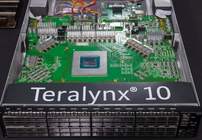
Here is the switch overview. We will work our way from the OSFP cages (right) to the power supplies and fans (left.)
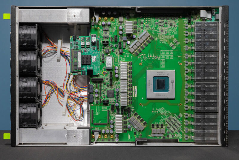
When we opened the switch, the first thing your eye is drawn to is the large heatsink.
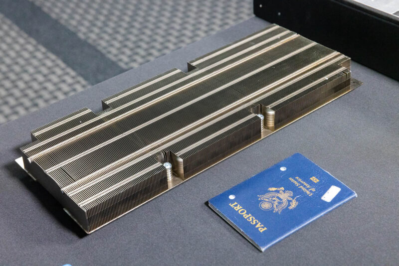
Here is the heatsink with an expired passport for scale.
Here is a bottom view of the heatsink.
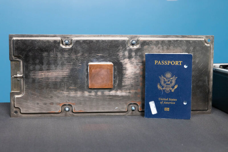
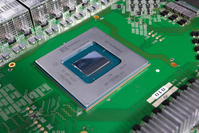
The chip itself is a 500W 5nm part.
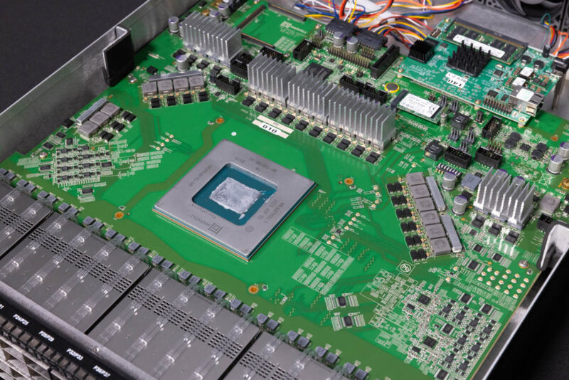
Marvell let us clean off the chip to get some photos without the heatsink.
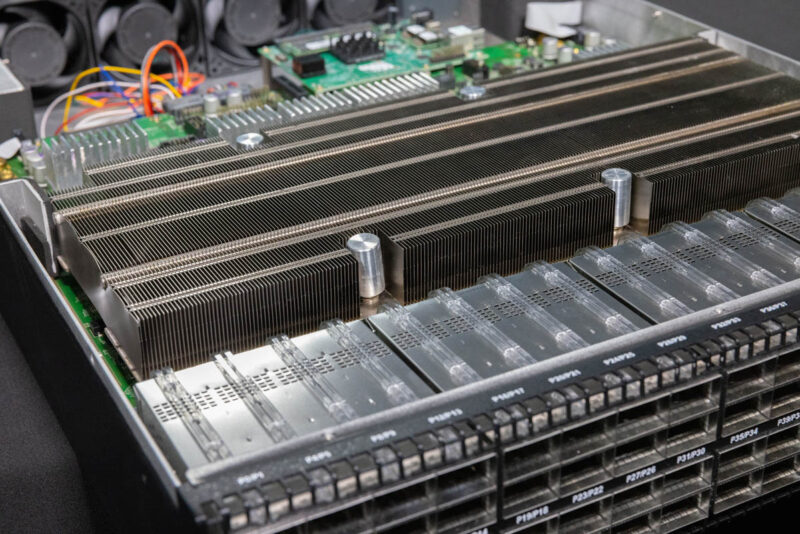
We could get a good look at the heatsink-less OSFP cages with the heatsink off.
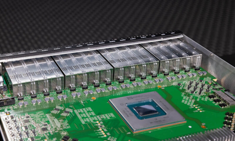
If you look at this view, there are only 32x OSFP cages. That is because the switch PCB is in the middle of the two blocks.
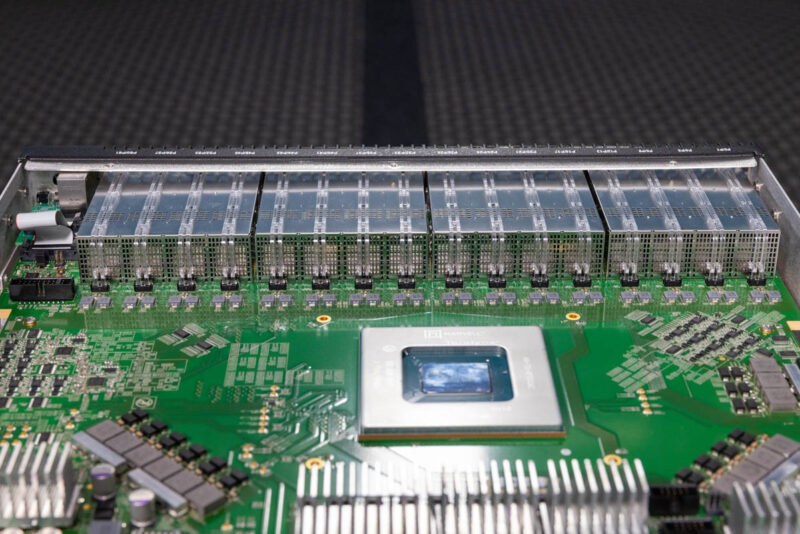
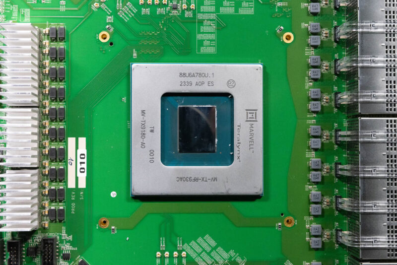
Behind the OSFP cages, we have the Teralynx 10 chip.
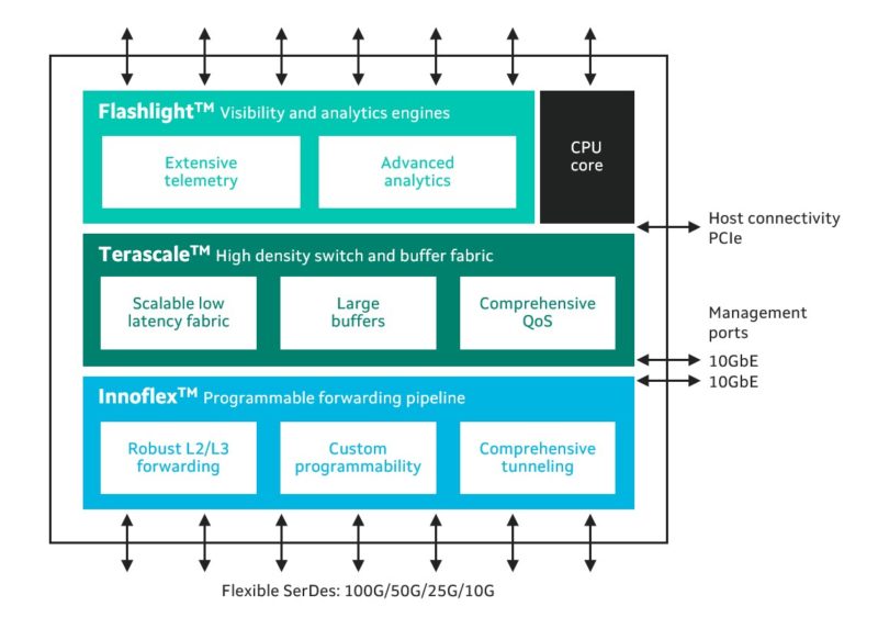
We will let folks read more about Teralynx 10 at their leisure, but here is the early functional diagram that we have shown before.
Something a bit different was that many of the components on the switch were at an angle and were not horizontal or parallel to the switch chip’s edges.
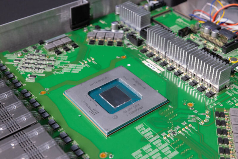
Here is a shot from above. This, again, is a 64-port 800GbE switch chip. If you come from the server world, we will get 800GbE single port NICs in the PCIe Gen6 era and have 400GbE PCIe Gen5 x16 NICs today. This chip has enough capacity to handle 128 of the fastest PCIe Gen5 400GbE NICs today.
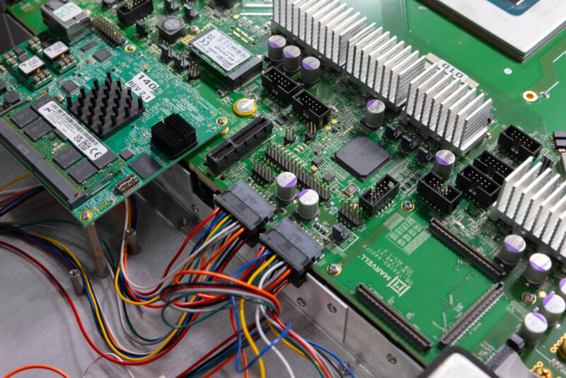
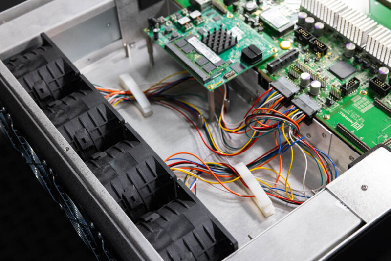
Like many switches, this Teralynx 10 switch has a dedicated management controller. Something fun here is that this is a Marvell Octeon-based management board. We were told that others can use x86 as well.
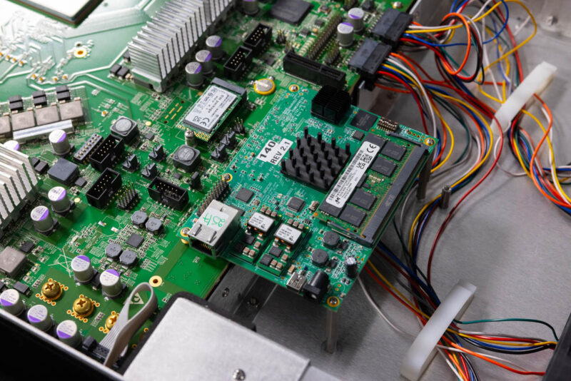
The M.2 SSD sits on the main switch board.
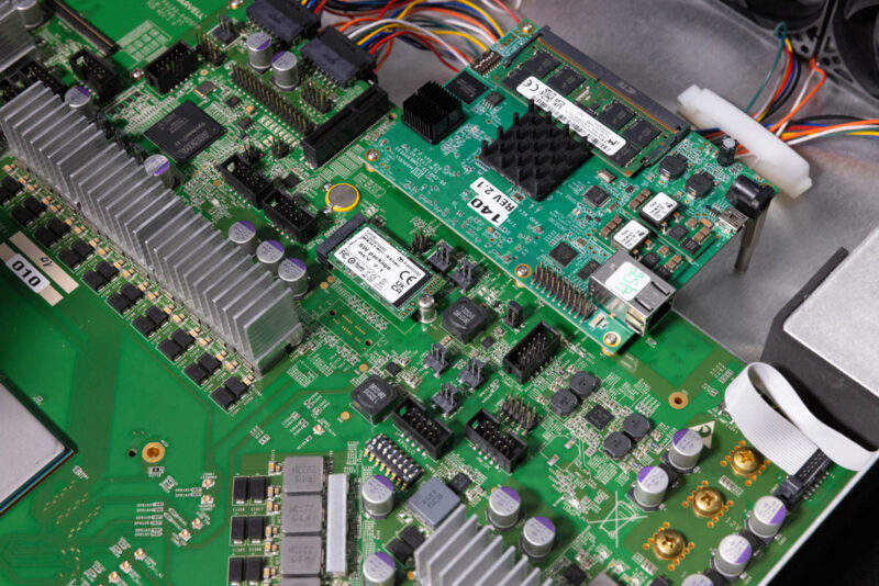
Something fun that we found was a built-in PCIe slot for diagnostics.
Just under that though, is a feature that you might easily miss. There is apparently a 10Gbase-T port exposed internally as a management interface.
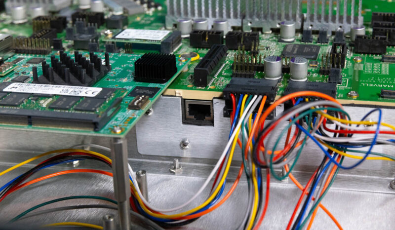
One other area to look at is just how thick the switch PCB. If a server motherboard was this thick, many 1U server designs would have extreme cooling challenges.
On the subject of cooling, we have a fairly straightforward fan setup with four fan modules at the rear of the chassis.
Next, let us head to the lab and see these running.


We’ve got a B200 cluster planned. Maybe we’ll see if a Marvell switch works then. It’ll depend on what NVIDIA also comes to the table with as it’s a cluster in the theme of thousands of B200s
I’m a fan of showing all this networking gear.
My only wish is that these types of speeds hurry up and make it into the lower power consumer space!
How can it be, that those fans are not hot swappable? We are talking about ultra high end hardware?!