
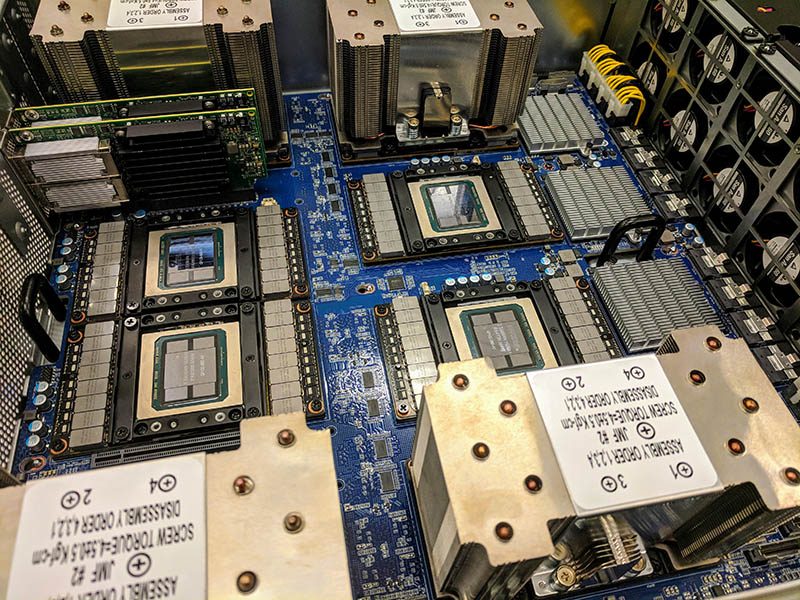
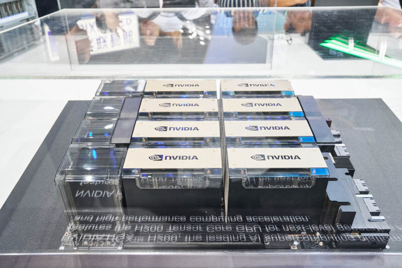
At Computex 2024, our team saw something that is really interesting. A bare NVIDIA HGX B200 board in the Ingrasys booth. Ingrasys is a division of Foxconn that may or may not be also heavily involved in the GB200 NVL72 build. In the company’s Computex 2024 booth, there was a NVIDIA HGX B200 board without its heatsinks, and that showed a big change. The NVIDIA NVLink Switch chips (no longer called “NVSwitch”) have reduced in quantity from four to two, and moved on the HGX baseboard.
NVIDIA NVLink Switch Chips Change to the HGX B200
As a quick history lesson on the 8-GPU baseboards from NVIDIA, we need to start with the P100/ V100 generation. In that generation, we would have PCIe switches on an 8-way SXM baseboard. There was NVLink between GPUs, but the switches were PCIe. Back when we did DeepLearning12 in 2018, we had to install our own heatsinks, and the baseboard was made by Gigabyte.
That DeepLearning12 build cost a lot. For example, we had to get a $350 torque driver that could hit the tolerances needed not to crack the NVIDIA P100 GPUs. I was in the data center starting to install these, and one of our kind readers who worked on the Baidu AI research cluster in that same data center stopped me, letting me know I might break the GPUs if the torque was not perfect. Indeed, the worst story I heard about this was that HPE broke several V100 generation GPUs due to torque/ thermal paste thickness.
One of the next big advancements came with the NVIDIA HGX-2 board. Instead of allowing board partners to make the baseboards and then install the cooling solutions, NVIDIA did all of this pre-integrated with its NVLink Switch chips, which were then called “NVSwitches.” Here, you can see the relatively small heatsinks required in the NVIDIA V100 era.
Moving to the NVIDIA A100 era, the NVLink Switch/ NVSwitch heatsinks got larger, but the entire HGX A100 platform was built by NVIDIA, and sent to vendors pre-assembled. Note, we are focused on the 8-GPU baseboard, not the “Redstone” 4-GPU baseboard that we reviewed in systems like the Dell EMC PowerEdge XE8545.
When it came to the H100 generation, we got better ducting around the NVLink Switches and GPUs, but as you can see, the four NVLink Switches are at one end of the HGX H100 baseboard.
Now for what we saw at the Ingrasys booth at Computex 2024. First, there was a NVIDIA HGX H200 baseboard.
This seems to follow the same design as the NVIDIA HGX H100 8-GPU baseboard with the NVLink Switches simultaneously.
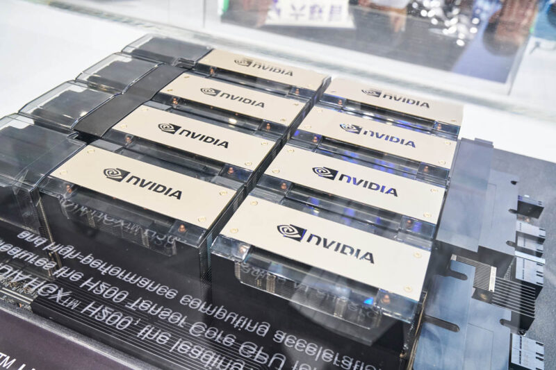
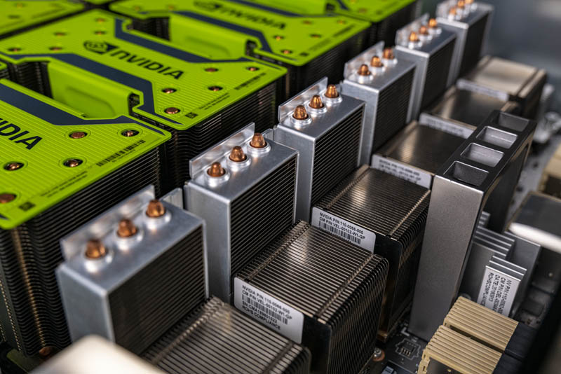
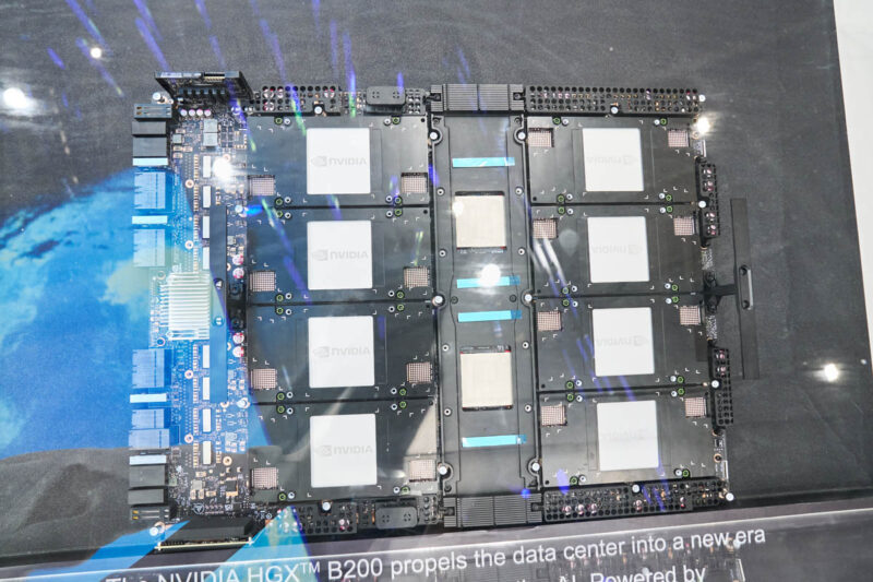
At the show, we saw the 8x GPU NVIDIA HGX B100 platform with even more NVIDIA branding.
For a better view, here is the same HGX B100 platform from the launch.
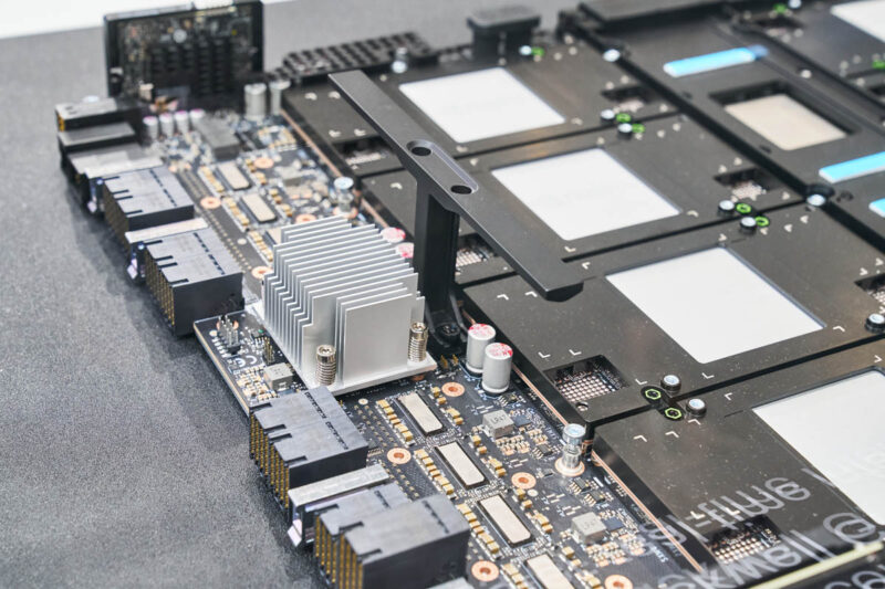
Something to note, though, is that near the edge connectors, we have PCIe retimers, not NVLink Switches.
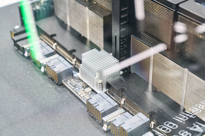
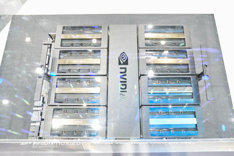
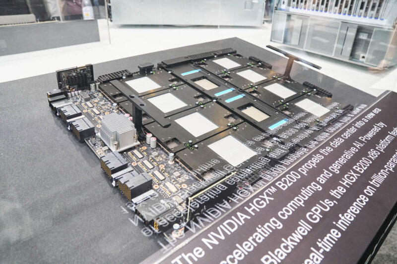
While there was not a bare NVIDIA HGX B100 board, there was a NVIDIA HGX B200 board without heatsinks. We asked NVIDIA, and the NVLink Switch setup should be the same.
Here we can see the PCIe retimers uncovered from their heatsinks. These tend to have smaller heatsinks since they have TDPs ranging from ~10-15W, depending on if you are talking about Astera Labs, Broadcom, or Marvell versions that use this footprint.
Something that stands out, is that the NVLink Switches are in the middle of the board, not the edge. There are also two not four onboard.
We asked NVIDIA to confirm these are the new NVSwitches, we received this response via e-mail “We haven’t disclosed the positioning of the chips, but we did go from 4 chips to 2.” At the same time, the company also corrected our branding when we called those two “NVSwitches” since “… the two chips in the middle are called “NVLink Switch” chips.
While NVIDIA has not disclosed the location of the NVLink Switch chips, there are two of these chips in the middle of the HGX B200 baseboard, and it was also confirmed on the HGX B100.
Final Words
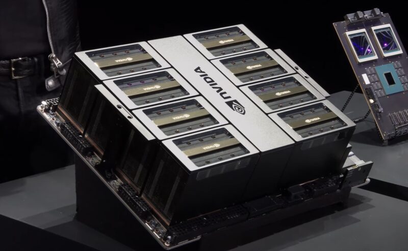
The NVLink Switch chips are bigger now and moving them to the center of the board likely reduced trace lengths versus having them all at one end. That has benefits when doing high-speed signaling. Further, the NVIDIA B200 GPUs have the sets of four GPUs flipped on either side, so it is likely NVIDIA also is doing that to further reduce trace lengths to the NVLink Switches.
It was great getting to see this at the show.


 and reposition them for shorter trace lengths)
This section could probably be reworded:
“Something that stands out, is that the four NVLink Switches are in the middle of the board, not the edge. There are also two not four onboard.”
Maybe:
“Something that stands out, is that the NVLink Switches are in the middle of the board, not the edge. There are also two not four onboard.”
Luckily the wrench was only $350!
https://www.mountztorque.com/FGA-80-Adjustable-Torque-Screwdrivers?quantity=1
ISO 16047:2005 and ISO 6789-1:2017