
At Hot Chips 2024, IBM went into its Telum II processor and Spyre AI chip. We typically cover IBM mostly at Hot Chips, but IBM is still making CPUs. We last looked at the IBM Z Telum Mainframe Processor at Hot Chips 33. It is great to see what is new.
Please note that we are doing these live this week at Hot Chips 2024, so please excuse typos.
IBM Telum II and More Processor and AI Updates at Hot Chips 2024
IBM Telum II is the next-generation mainframe processor from IBM
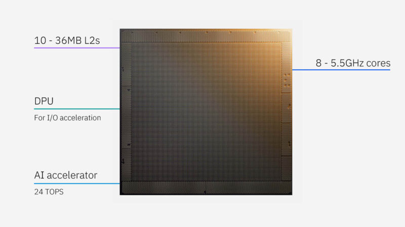
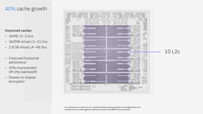
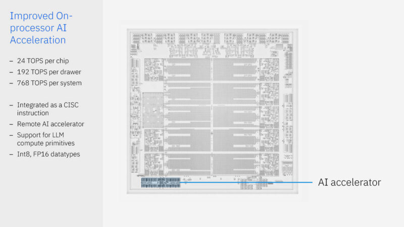
Here are some of the key items from the chip. There are ten 36MB of L2 caches with eight 5.5GHz cores running fixed frequency. There is also an onboard AI accelerator at 24 TOPS. IBM has a “DPU” integrated.
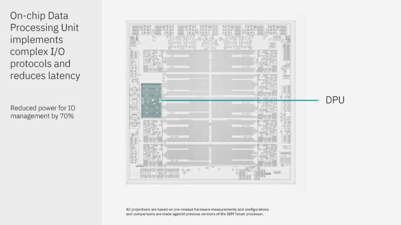
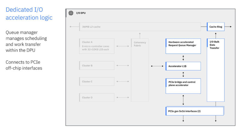
The DPU has to handle tens of thousands of outstanding I/O requests. Instead of putting the DPU behind the PCIe bus, it is coherently connected and has its own L2 cache. IBM says this increases performance and power efficiency.
Here is the DPU diagram. There are four clusters of eight microcontrollers. IBM runs its own custom protocols. The onboard DPU allows it to do so using these microcontrollers.
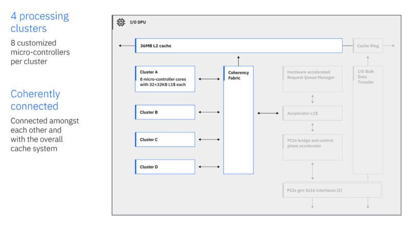
The DPU also has PCIe Gen5 x16 interfaces. IBM is running its own custom ISA and more in this DPU.
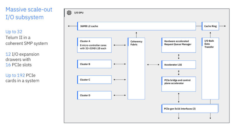
A full system can have up to 192 PCIe cards with 12 I/O expansion drawers and 16 PCIe slots eac.
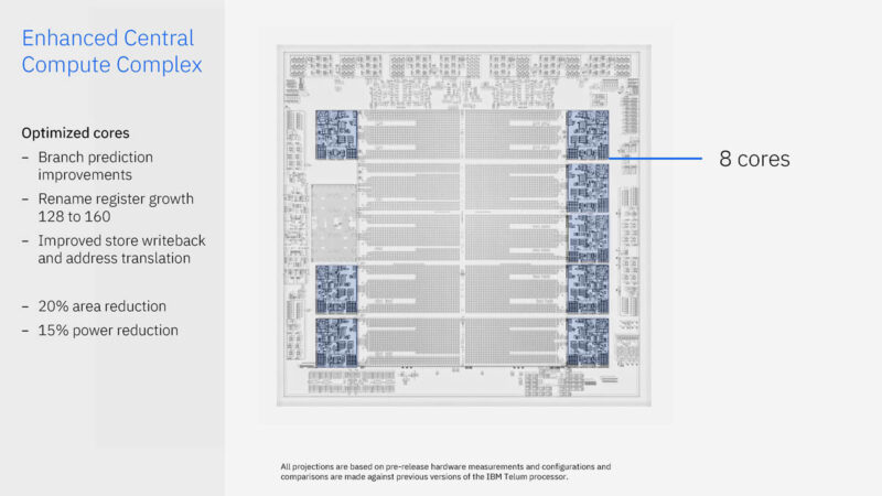
IBM did a revision on its cores as well. Something fun here is just how little of the floorplan is dedicated to the cores.
The ten 36MB L2 caches are fast, but there are more. There is a 360MB virtual L3 cache and 2.8GB of virtual L4 cache. IBM’s chips advertise the amount of free space in L2 caches and can use that cache elsewhere.
IBM is using Samsung 5nm. The cores run fixed at 5.5GHz.
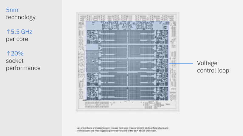
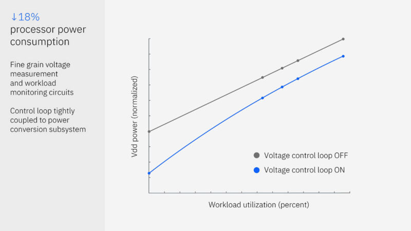
Telum II has a new voltage control loop that can help the cores run at 5.5GHz while workloads vary on the processors.
Next, is IBM’s AI performance.
IBM is designing its AI accelerator specifically for its enterprise clients.
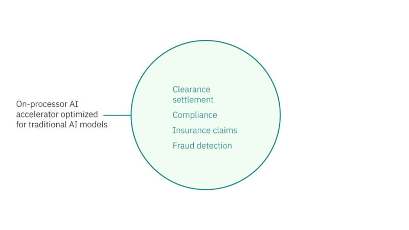
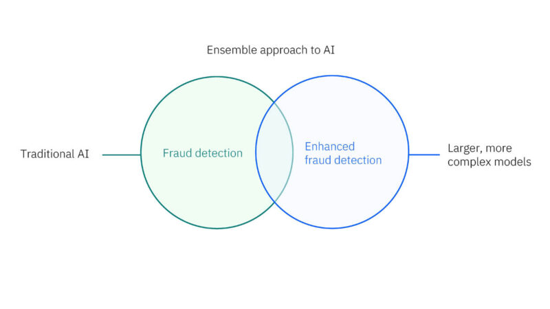
IBM Spyre for optimizing the use of large and small models with different accuracies.
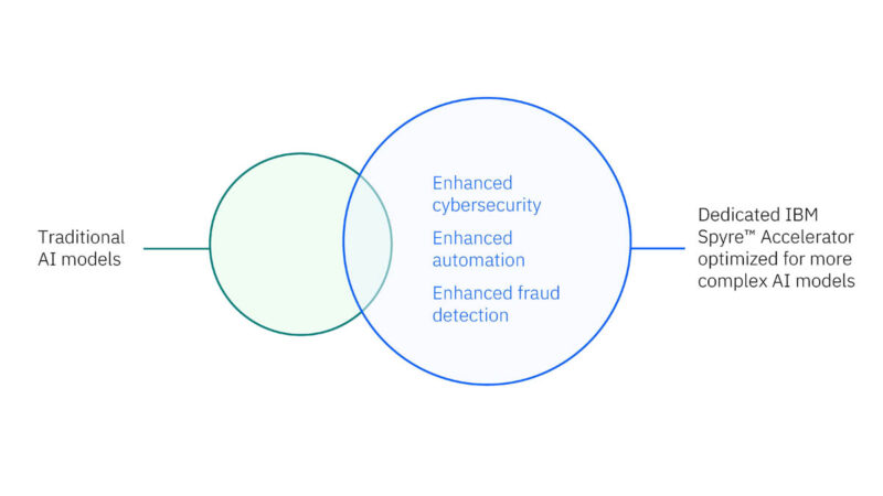
For example, the traditional small, efficient models for fraud detection, in addition to the larger models for certain transactions, are becoming more common.
Telum II implements the on-processor AI acceleration as a CISC instruction while the accelerators are doing compute.
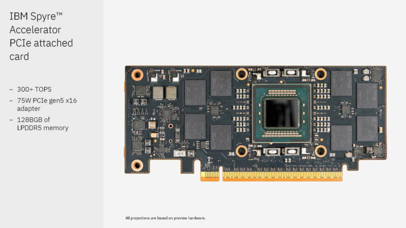
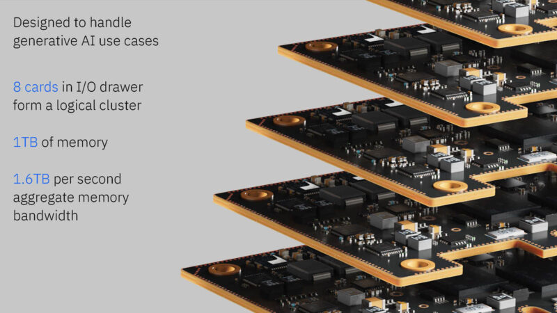
Here is the IBM Spyre Accelerator PCIe card. These cards have 128GB of LPDDR5 memory and run at 300TOPS and only 75W. This is for things like LLMs where the models are so large they do not fit on the processor chips.
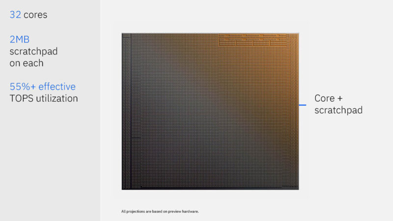
Here is the chip. Each of the 32 cores has 2MB of scratchpad, which is to hold data but is not a cache. As such, IBM does not need a standard cache management system.
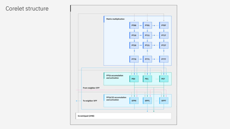
Here is a look at the processing tile.
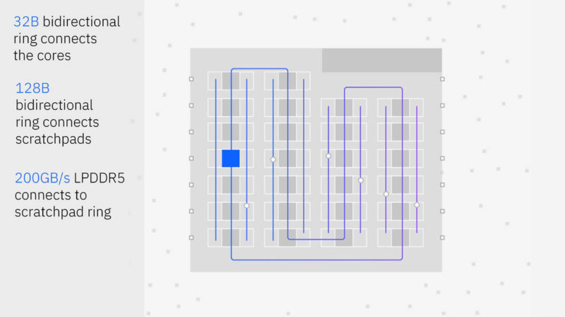
There are multiple fabrics on the chip.
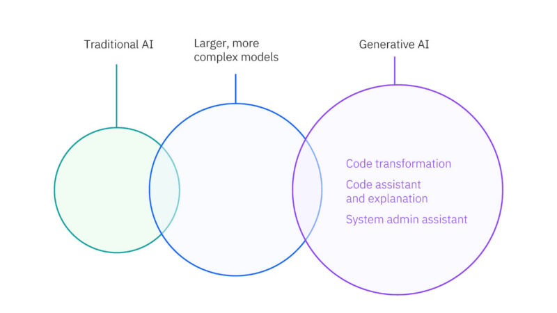
IBM has been looking at predictive AI, but it is also looking at generative AI on Spyre.
Each drawer with eight cards gives 1TB of memory across the cards.
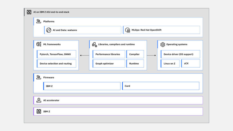
Here is the AI on IBM Z software stack.
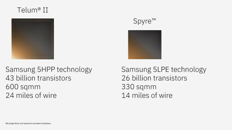
Both Telum II and Spyre are built on Samsung 5nm, but use different process versions. Here are some of the specs:
This is always very cool.
Final Words
IBM says that a test IBM Z system with 96 Spyre cards can hit up to 30 PetaOps of performance. These are very different chips designed for a very different use case. Reliability is key, and the engineering for providing performance gains while handling I/O and maintaining reliability is super cool.
One day, reviewing an IBM Z system and taking one apart would be a lot of fun. We can hope.


Telum II is a bit of a let down. The first generation had a novel virtual L3 and L4 cache topology so my expectation here was that IBM would move to leverage 3D stacking to increase cache count as historically Z series loves cache. In fact, my personal expectations was zero L2 on the die but a rather large L1 data cache.
The rest of the die space on the primary die would be to increase core counts and various accelerators. That did happen to an extent, though it seems IBM is rebranding some of the features that already existed on the Z platform as a DPU. Historically IBM has had numerous service processors to handle such networking and storage tasks to keep the main CPUs free: mainframes are all about delegating as much work off of their main processors as possible. These are fully cache coherent and have their own slice of L2 cache which is noteworthy compare to previous implementations.
I am also hyper curious about this systems IO capabilities. I was pondering if this platform would be the first to go CXL only for main memory. IBM already deployed a serialized memory buffer but it did not share capabilities with PCIe. With would’ve provided some flexibility between IO performance and memory capacity, a very interesting thing to balance on a mainframe and given customers a choice.
@Kevin G I disagree with you. A bit down? +40% cache growth, +20% performance, 20% power reduction, increased frequency… is impressive. At least for me. Note that they did not play the “trick” to add more cores and evaluate cpu-bound high parallel workloads like other vendors do. I think that IBM engineers optimized quite a bit their previous design… yeah, I agree maybe not many uarch innovation announced, but they got quite a bit of improvements optimizing and polishing the rest, huh? Not only that, they also increased significantly AI capability (is it what their customers demand? are we going to have personalized genAI in our bank accounts? haha) and the I/O capability (this is probably related to what the new AI workloads demand). I miss more technical details but overall looks like they got it again… I’m a big fan of this technology. It is a testament of good engineering and adapting to their customers needs. I’m looking forward to the upcoming technical conferences when they typically unveil some more details. You are right, Z had what they called system assistant processors (SAPs) or something like that, that were CPU cores reserved to offload some systems tasks (typically I/O but also others). I guess that now with a DPU integrated in every chip, maybe there is less need for SAPs (increasing computing power?) or maybe some I/O just go to the DPU directly and is processed in parallel (not in a single-threaded general purpose big core), reducing latency/increasing throughput/saving power as they claim. Another benefit seems that the DPU is programmable, so probably they can implement all their super reliable custom protocols in firmware rather in specific cards beshing the PCIe interface… I’m looking forward to what Telum III will look like! ;)
@Patrick: “One day, reviewing an IBM Z system and taking one apart would be a lot of fun. We can hope.” Getting a current Z system from IBM for review AND getting permission from them to take it apart would be the scoop of the decade!