Why settle for 400GbE networking in 2024, 800GbE networking next year, or 1.6Tbps networking in 2026? Enfabrica has an 8Tbps SuperNIC at Hot Chips 2024.
These articles are being done live at Hot Chips 2024, so please excuse typos.
Enfabrica ACF-S An 8Tbps SuperNIC at Hot Chips 2024
Enfabrica was started in 2020 to solve high-end networking.
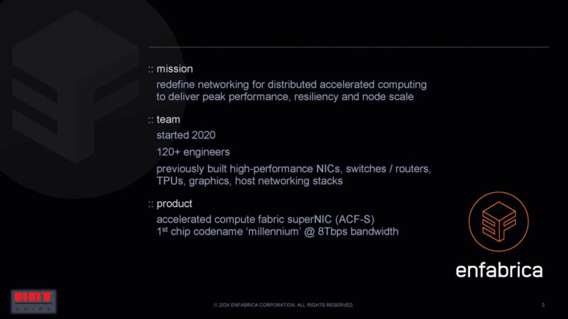
We are starting with looking at scaling compute across different chips. First, we have a coherent memory system working in a big system, such as with mainframes. Latency could be managed because the transport was built by a single vendor.
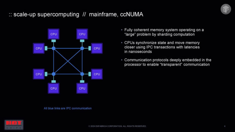
Then, systems started to scale out, so we got things like the standard Ethernet networks we all use.
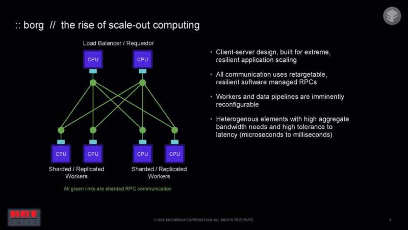
Now we have a combination of scale up and scale out for huge AI clusters and similar topologies.
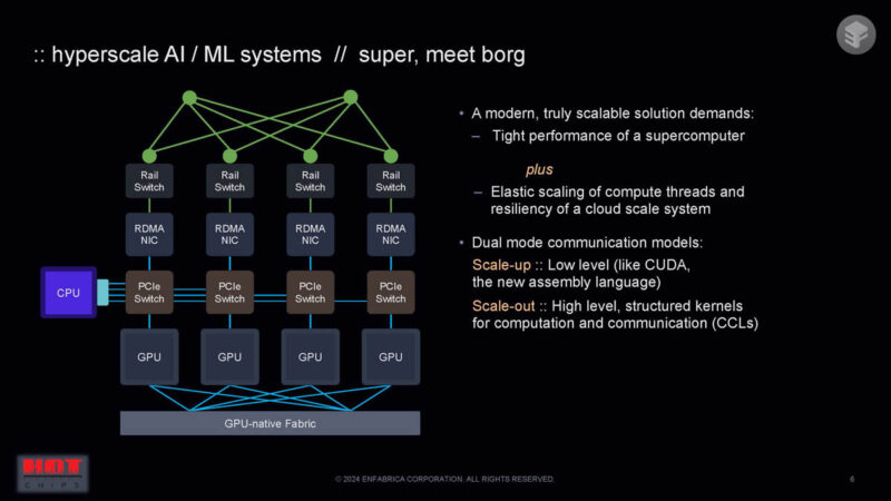
Scaling both the scale-up and scale-out domains is challenging for fabrics. Modern AI systems are very large.
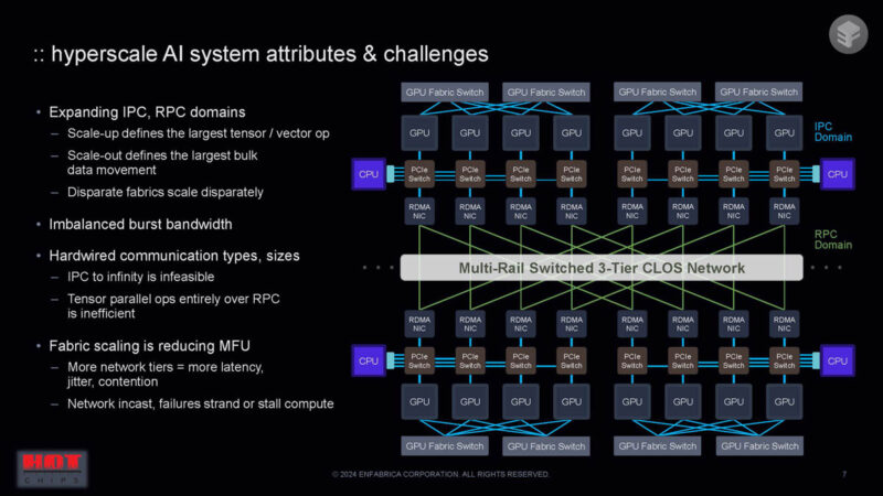
The idea behind Enfabrica ACF-S seems to be using scale-up and scale-out interfaces and has high-bandwidth domains for both IPC and RPC domains. It can drive communication to the optimal path.
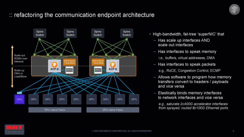
Something that is very different is that you could create a network that looks similar to today’s PCIe switches. This is not a PCIe switch, however.
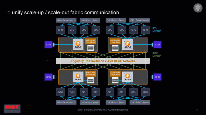
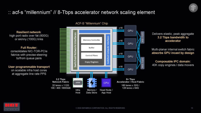
Something big in the Enfabrica ACF-S “Millennium” is that it is designed to ingest multiple GPUs or AI accelerators, GPUs, and more and run them through one large chip. This is a big data mover chip.

Data movement happens through crossbars and virtual queues plus through multi-banked buffers.
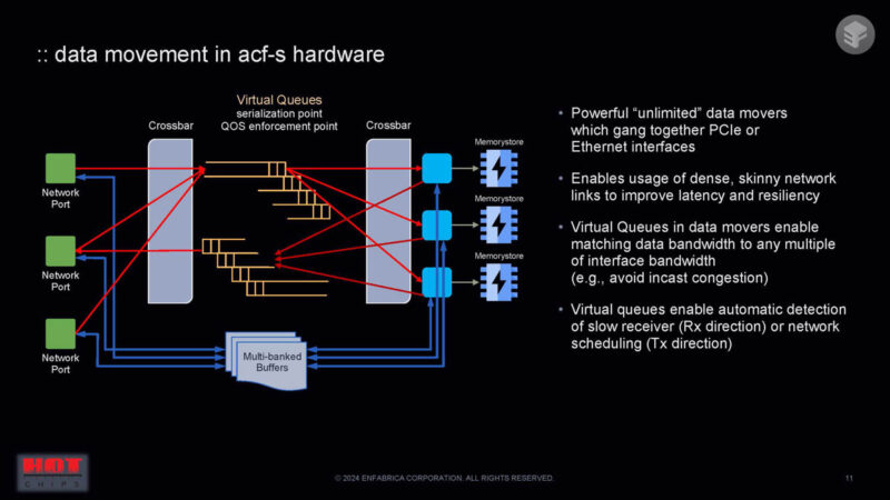
The infrastructure CPU using descriptors can define the memory shape, bytes of header, and the networking policy, and deliver hardware on both the IPC and RPC side. There is a lot more on the slide, and this talk is going really fast.
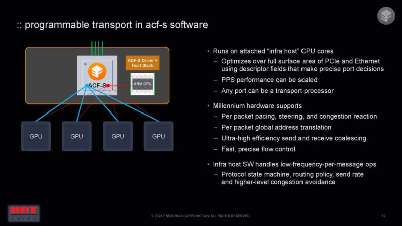
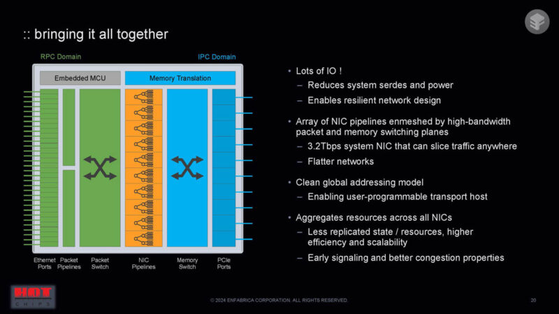
Here is a block diagram on the left with 32 lanes of 100GbE. That feeds into the switch. The NIC pipelines convert from the NIC work to the memory world. There is then a memory switch and PCIe ports.
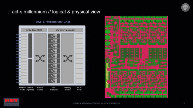
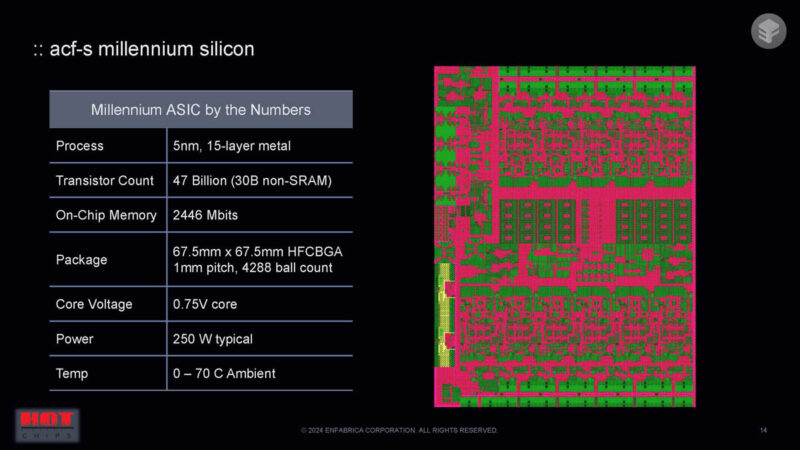
This fabbed in 5nm with a lot of I/O.
Here are the differences between this chip, and other NICs.
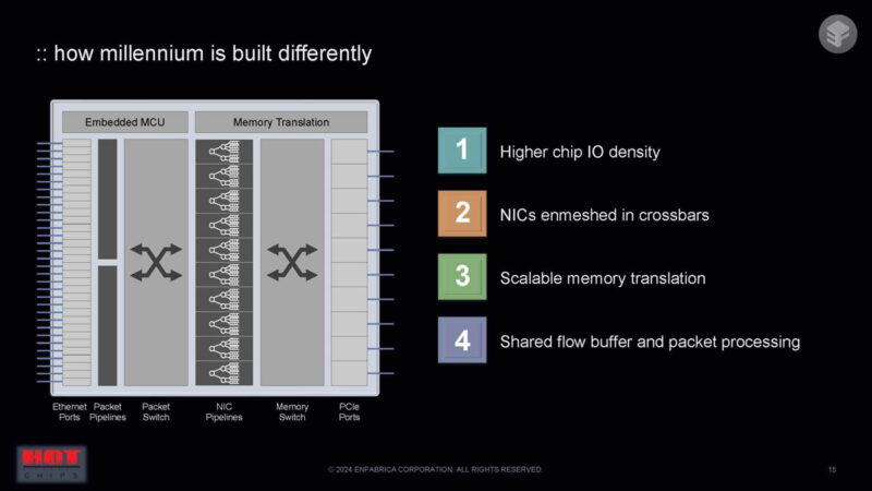
Instead of a NIC being simple memory on one side and a network on the other device, Enfabrica changes this to a many-to-many. It iss very cool that this also supports CXL.
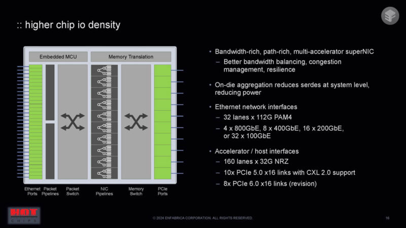
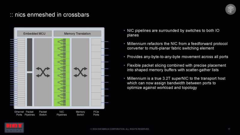
The NIC pipelines are surrounded by crossbars on either side and operates as a giant 3.2T NIC.
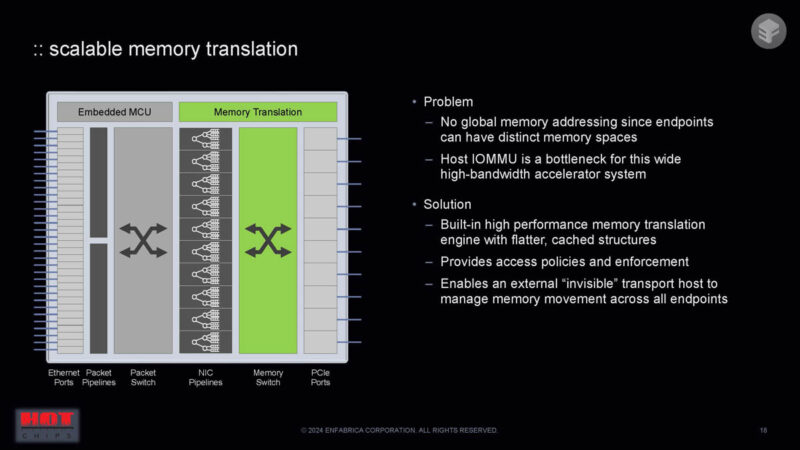
There are a few challenges with building something this big. One of them is around handling memory translation.
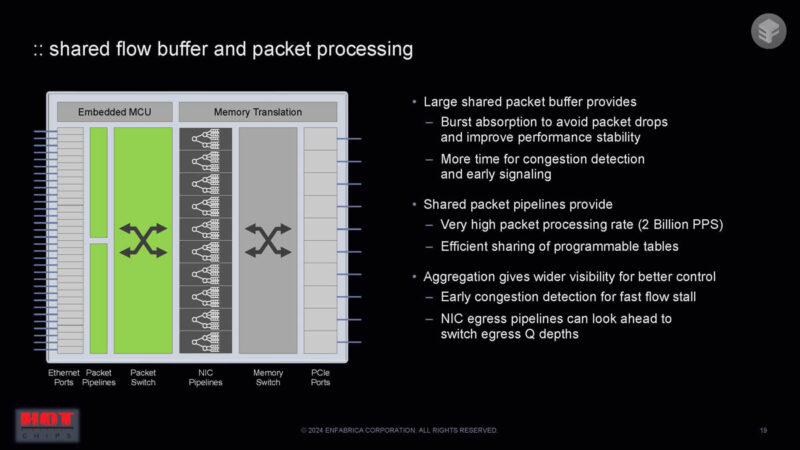
Here is more on the shared flow buffer and packet processing features.
So, bringing this together, this is a 3.2T NIC with lots of I/O. Instead of having several NICs separately, the larger NIC adds features by moving the aggregation points from PCIe switches and network switches to a larger single NIC device.
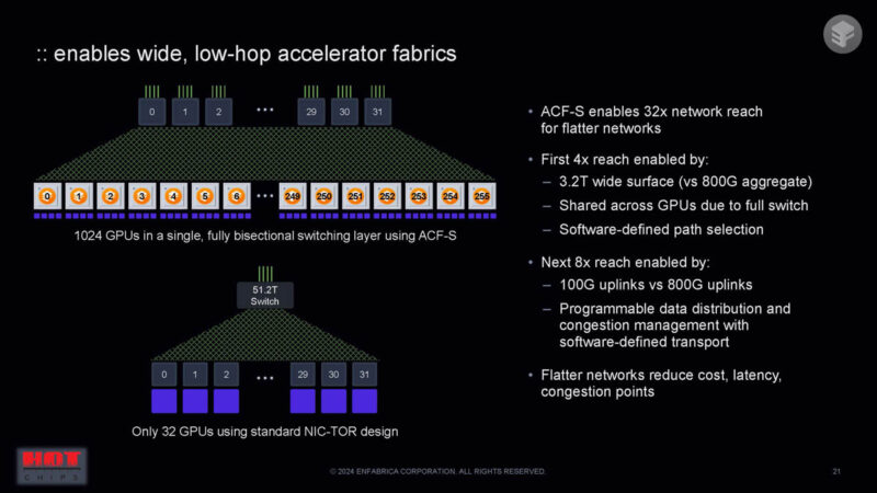
One of the big benefits is that in a single switch layer one can get to 1024 GPUs instead of 32.
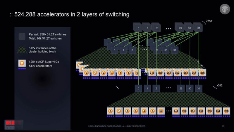
A huge benefit is that the radix of the device can lead to 524288 accelerators on a 2 layer switched network.
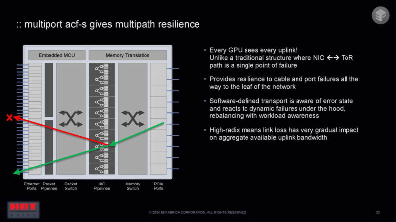
The links are resilient because multiple links from the GPU to the network exist. If a link fails, the GPU might see a performance blip, but the packets would find another path which can be better for reliability.
Here is the summary slide.
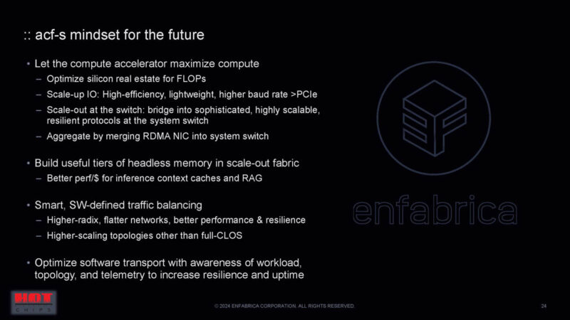
Very cool.
Final Words
I love this. It is like taking a bunch of NICs and combining them, and PCIe switches, and combining all of these into one. The other interesting use case is that one could add CXL memory to the ACF-S fabric and present pools of CXL memory without hosts. This is super cool. Hopefully we start seeing these soon.

