Earlier this week we covered Marvell Nabbing a Big Multi-Year Multi-Product Win at AWS. Not to be outdone, Broadcom is announcing its new 3.5D XDSiP technology for next-generation XPUs that are planning production in 2026. As a cool bit here, Broadcom says it is the first to use Face-to-Face 3.5D stacking. AI is driving chips to get bigger and therefore co-packaging more components. As a result, packaging is going to be a big deal in the future.
Broadcom 3.5D XDSiP with Face-To-Face 3.5D For 2026 XPUs and Beyond
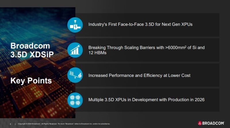
Here is the overview slide for the announcement. One that should get folks excited is that the company is looking at integrating over 6000mm2 of silicon and 12 HBMs in this design.
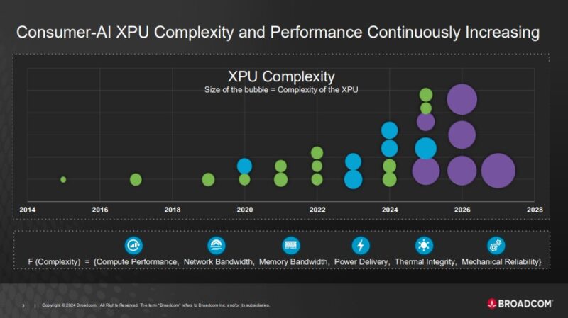
Something that we know is that XPUs are becoming more complex.
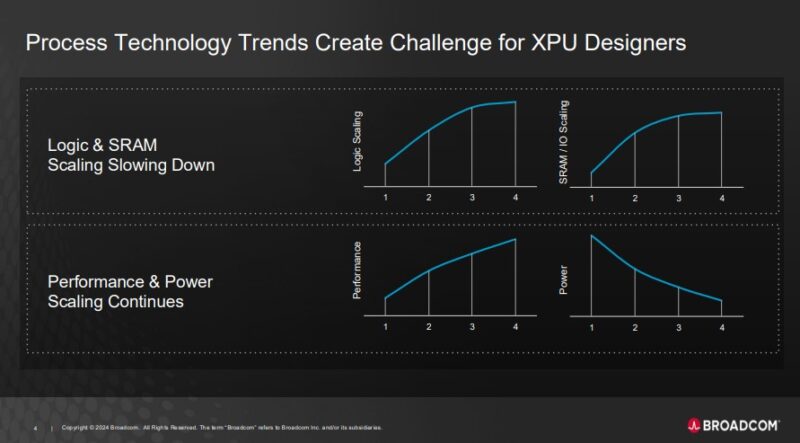
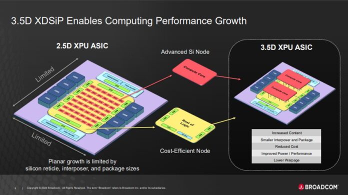
Part of the reason for co-packaging is that logic and especially SRAM scaling is slowing down. So co-packaging multiple pieces of silicon allows for the best process nodes to be used for each part. It also allows one to make larger chips.
As part of the 3.5D XDSiP packaging, Broadcom envisions moving the compute cores off of a logic tile. Instead, those compute cores can be built on a leading process node. The rest of the logic, and links for HBM, die-to-die interconnects for things like PCIe and 100GbE/ 200GbE chiplets, and high-speed SerDes can be on a different logic die, albeit one not on a leading process node.
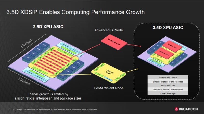
Part of the idea here is that only using the leading process for the highest-impact compute cores is a more cost-efficient way to design chips. Broadcom also says that it can reduce warpage which is a big challenge in modern multi-tile processors since different tiles and nodes heat and expand at different rates.
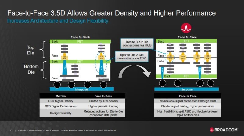
One of the big innovations is that Broadcom is using Face-to-Face 3.5D. This allows dies to have direct HCB connection points without having to traverse Thru Silicon Vias or TSVs. As a result, chip designers can get higher-density tile-to-tile connections for more throughput and design flexibility.
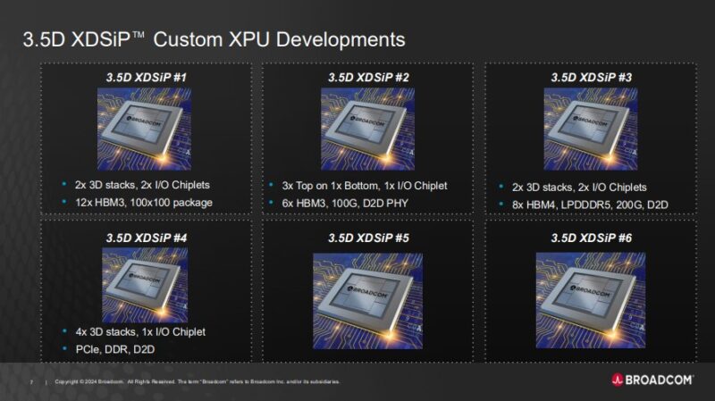
Broadcom also says that it has a number of different designs for customers using this technology. Here are six of them, four of which have some stats alongside the chip wins.
This is still a future technology, but one that is in the 2026 production timeframe making it <2 years from reality.
Final Words
Packaging larger chips is one way to get significantly better system efficiency. With AI clusters, moving off chip/package to another chip is useful to expand the memory pool for a given problem and add more compute resources into a job. The challenge with scaling in this manner is that driving signal off package requires a lot more power while adding cost for optics, DACs, and sometimes retimers. Making larger chip packages means that the resource aggregation has fewer of these off-package links to hit a given level of performance. It is a key building blocks to scale massive AI buildouts in a power-constrained environment.
Now we just want to see these with CPO!


Hey Broadcom, that’s not how dimensions work. Slapping an extra layer on a 2.5D chip does not make it 3.5D.
So this is like AMD’s 2023 MI300-platform?