Bolt Graphics Zeus Architecture
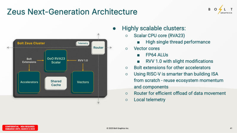
We are not getting a full block diagram yet, but this is a RISC-V RVA23 out-of-order scalar core. There are then vector cores and accelerators. Something that is at least slightly reminiscent of some other startups we have seen is the use of RISC-V. Instead of building its own ground-up ISA, it can use RISC-V plus then add its own special sauce.
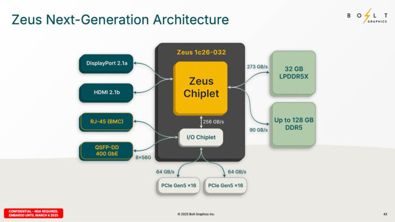
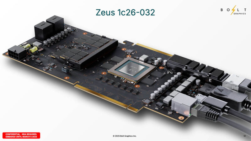
It feels a bit like the Zeus 1c26-032 is a single chiplet part. We have DP 2.1a, HDMI 2.1b, and then some really neat features. Namely, there is a RJ45 BMC port as we have seen on DPUs, servers, and other components, but less commonly on GPUs. There is a QSFP-DD port for 400GbE, and two PCIe Gen5 x16 slots. Bolt Graphics can apparently do PCIe Gen5 / CXL 3.0 and Ethernet for a lot of flexibility. On the memory side, there is 32GB of LPDDR5X and up to 128GB of DDR5. The LPDDR5X here is being used because it is cheaper and higher capacity than either HBM3 or GDDR7.
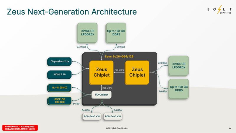
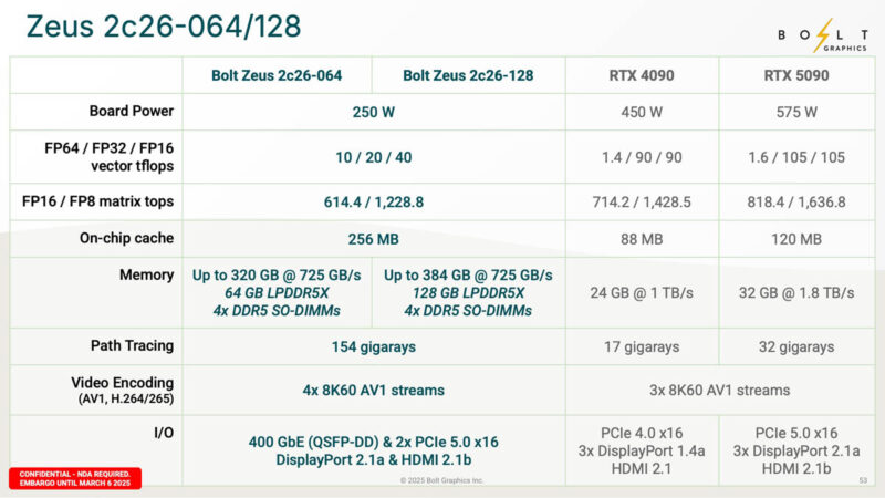
The Zeus 2c26-064/128 is the two chiplet module. The 64 or 128 seems to be the capacity of the LPDDR5X.
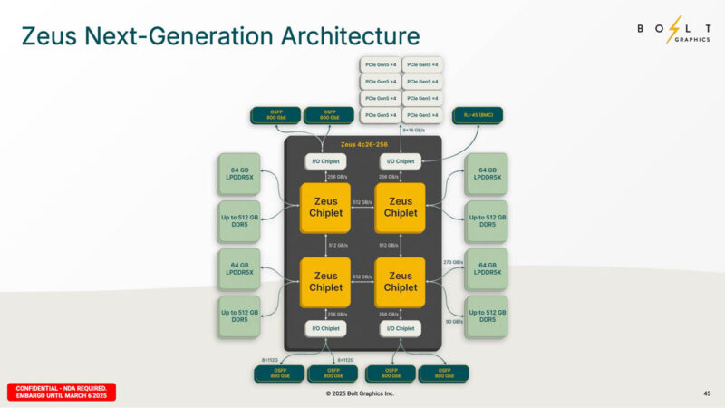
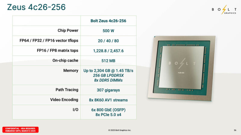
Scaling up, and very interesting here, is the Zeus 4c26-256. Each chiplet gets an I/O chiplet and 64GB Of LPDDR5X. So there is a lot of OSFP 800GbE connectivity along with PCIe Gen5 and memory. Something to keep in mind here is that we often say that PCIe Gen5 x16 is around a 400GbE port. So with two Gen5 x16 ports, and the ability to do either PCIe/ CXL or Ethernet, that seems to track the diagram here. With 256GB of LPDDR5X and 512GB of DDR5 DIMMs per chiplet for 2TB, that gives us the 2.2TB of memory total on the GPU.
Taking a look at the smaller chiplet, this is the Zeus 1c26-032 card. You can see the two DDR5 SODIMM slots on the card as part of the expandable memory.
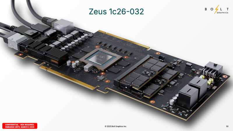
We can also see the BMC port, HDMI port, DisplayPort, and the QSFP-DD 400GbE port.
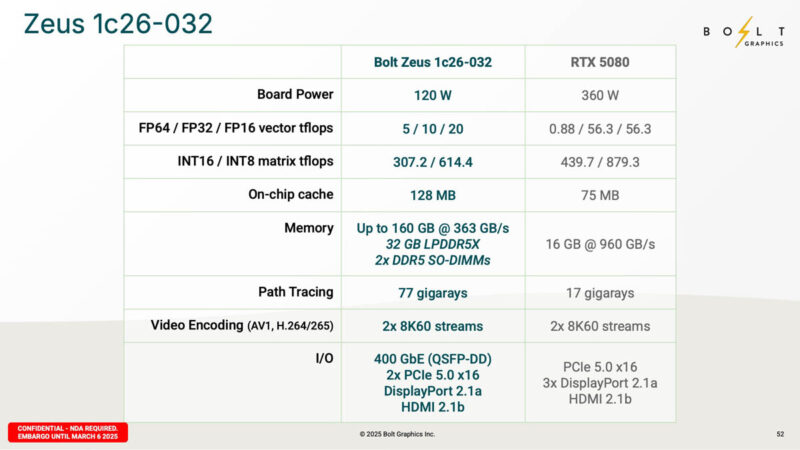
Here are the specs. We can see that Bolt is aiming at a relatively lower power envelope and has more local cache.
Here are the specs on the larger 2c26 platforms. Worth also noting here is that Bolt Graphics is targeting lower memory bandwidth, but higher memory capacity in its designs.
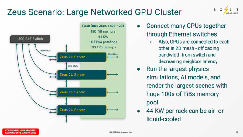
Taking a step back on the big 500W Zeus 4c26 part, the 6x 800GBE is really interesting. That is a lot of connectivity coming out of a GPU. Putting that into perspective, that is ~12x PCIe Gen5 x16 lanes worth of bandwidth. It also means many fewer NICs being sold since these GPUs have them built-in.
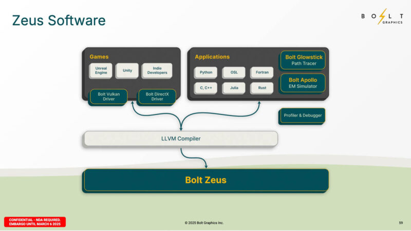
Software is going to be a big part of this. It feels like the Bolt Graphics folks have a vision, but they need to work on the software side.
It also feels a lot like these are less meant to be deployed as a single GPU in a system, and instead are designed to be clustered. A small cluster might be two GPUs.
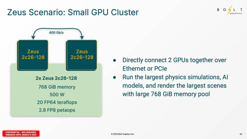
Adding a switch would mean a large memory footprint in a smaller power budget.
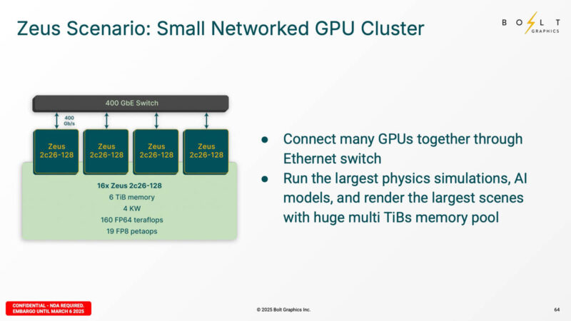
On the larger scale, the goal is to scale-out using 800GbE. We have looked at 800GbE switches like the Marvell Teralynx 10 51.2T 64-port 800GbE switch and this year we will have the 102.8T switches for 128x 800GbE links.
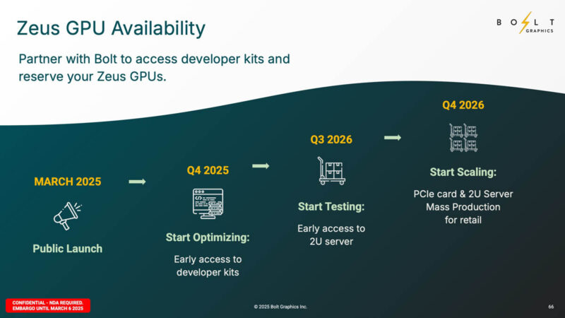
In terms of availability, early access to developer kits is scheduled for Q4 2025 and then scaling in Q4 2026. That gives folks like NVIDIA quite a decent amount of time to react if they feel it is necessary.
For our readers, it looks like maybe we will see more of these in the future.
Final Words
This feels like an announcement where we really want to see product. The fact that we are still a few months away from early developer kits makes this feel a bit early. On the other hand, if Bolt Graphics has Zeus competing with a combination of NIC and consumer GPU, while offering more memory then it could be a really neat combination. I am always a bit skeptical of products until we see them live. Hopefully, we can show you this in action as the hardware becomes available.


The general sentiment is that if “Bolt graphics” had anything revolutionary, they would have been bought out by one of the major players.
They’ll be at Hot Chips, and maybe they’ll have something real to show by then. Lots of big promises and marketing fluff so far.
The marketing looks attractive to me in that they claim enough tflops and memory bandwidth to be interesting. From my point of view it’s not just cost-power-performance that’s important but the software stack.
In that direction RISC-V inside sounds similar to the cancelled Intel MIC approach. If it works, then it might be significantly easier to program than the weird instruction set architectures used by current GPU accelerators
You can bring a gpu back from two decades in the future but if the software compatibility isn’t better than the current state of AMD’s then it’s gonna be tough to grab any meaningful market share.
Matrox is still making GPUs…
I have one question we should all be asking ourselves right now.
If a small startup can deliver 2.25TB of memory, why does NVIDIA limit us to 24GB on consumer GPUs?
If I were Bolt Graphics, I would focus my resources on developing and fine-tuning LLM-assisted coding to rapidly build a comprehensive software ecosystem that competes with CUDA, TensorRT, PhysX, G-SYNC, and NVIDIA’s SDKs. Their hardware already proves that NVIDIA, AMD, and Intel have been artificially limiting advancements, releasing minor upgrades while creating a false sense of scarcity.
The industry constantly pushes the narrative that hardware is never enough, keeping demand high while restricting access to more powerful configurations. Zeus GPUs show that a small company can deliver what the big players refuse to release. If Bolt wants to succeed, they must break away from hardware-first thinking and aggressively build the software foundation that will drive adoption.
First impression is very positive one, at least for me.
They are so different that they don’t really need to directly compete with nVidia/AMD/Intel etc.
If their thing allows some interesting generality aspects that dGPU can’t touch due to its uniform “many stupid execution units goose-stepping oover every problem”, they have a winner.
Looking at the performance examples they’ve chosen to share it’s clear that there’s extreme cherry picking for examples that are purely mathematical. Combining this with the small memory bandwidth as per the specs it’s pretty clear that these GPUs will suffer for any tasks where larger amounts of data or load/store operations are required.
Another red flag is the hyperfocus on hardware and barely mentioning software side of things (like SDKs, compatibility with common frameworks and applications etc.)
Isn’t this basically just Xeon Phi, but with RISC-V instead of x86?
Just goes to show you that NVIDIA, a $2.71T company is actually a B.S company that rips us off if a small startup company can easily develop a GPU with 2.25TB of memory.
We need more players in this competition otherwise we will suffer financially and as can everybody see, NVIDIA love’s money more than their tech anyway.
Anyone remember Bitboys Oy?
“Anyone remember Bitboys Oy?”
They might not have released the promised hardware, but they did have valuable people and IP. First ATI bought them and then later, when AMD had bought ATI, they sold the IP (Imageon) and team to Qualcomm…
Why would Qualcomm want it? Because Adreno is based on the technology. Not such a failure as you remember, now is it?
Color me skeptical. RiscV has put many interesting benefits on the table, but performance has yet to be one of them and doing chiplets at this scale with it is all new. I also doubt they will be able to use slotted memory and be able to keep timings in check with the parallel complexity that comes with a GPU.
I wish them all the best because competition in this area is desperately needed, and I also appreciate they are not using the AI gimic to gather interest that will ultimately amount to nothing. Hopefully that bubble pops some before this comes to market.
@gyges3D: GDDR @ max. 2GB / chip and max. 2×12 chips / GPU = max. 48GB per GPU. For its consumer-grade cards, NVIDIA only offers one chip per bus. The big three DRAM manufacturers are expected to launch 3GB capacities with GDDR7. Theoretically, they could go higher but they would rather sell HBM in the AI data center space.
NVIDIA’s Project DIGITS platform will be its first to use the slower LPDDR, much like Bolt. Note that Apple just announced a configuration limit of 512GB for the Mac Studio with M3 Ultra, so either they have 64GB LPDDR chips now or that platform uses a hybrid LPDDR / DDR memory architecture, as Bolt does. Stay tuned for the teardowns.
IIRC Apple’s earlier Mx chips had their RAM inside of the SoC, so tearing an M3 Ultra down may not tell anyone a whole lot. IIRC they’re claiming >800 GB/sec of memory bandwidth, which would be a *lot* of pins if they carried that externally.
Wikipedia says the M3 Max uses LPDDR5 6400, so there are presumably 16 channels under the hood to get 800 GB/sec, assuming they’re not cheating and the M3 Ultra is really 2x Maxes as advertised. That’d be 16x 32GB chips, right?
Is it known if it’ll use ECC RAM? Anything known about pricing?
@Scott Laird: Apple buys the LPDDR chips and includes them in its SOC packages, so you can clearly see them immediately adjacent to the central die after the joint heat sink is removed. Also, Apple uses 128 bit memory bus controllers and one chip per controller. 8 buses * 128 bits / bus * 6400 Gbit/s * 1 byte / 8 bits = 819,2 GB/s.
Until now, the capacity limit was 32GB / chip but Apple is now offering up to 512GB on the Mac Studio. So either they have sourced 64GB chips or they have changed their memory architecture.
This article would benefit from adding the tag: RISC-V
This CPU reminds me of STH’s article about “Ventana Veyron V2 RISC-V CPU Launched for the DSA Future”, but less.
@gyges3d March 6, 2025 At 10:21 pm
“I have one question we should all be asking ourselves right now.”
Watson Jr. memo about CDC 6600 ;-)
https://www.computerhistory.org/revolution/supercomputers/10/33/62
Anything in the GPU market sphere is welcomed. The more competition the better. I’ve had enough of the Ndiva dominance and pricing.