
In the world of GPUs, it has been NVIDIA, AMD, and Intel for some time. There are other projects in China especially, but companies breaking into the US market has been rough. Instead of just building low-end graphics and hoping to scale, Bolt Graphics is solving a specific challenge when it comes to high-end GPU computing and is doing so elegantly.
Bolt Graphics Zeus
Here is one of the craziest overview slides you will see for GPUs in 2025. It does not have a single mention of AI.
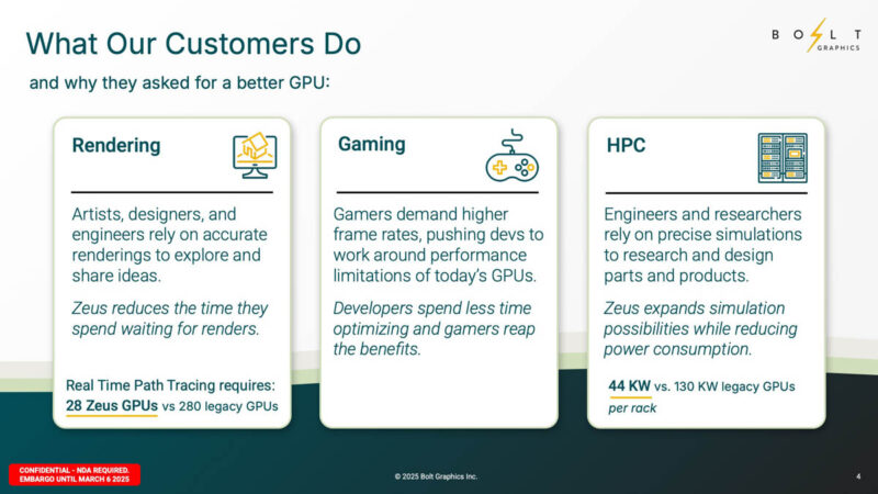
Instead, this is designed for rendering, gaming, and HPC. As you might be thinking, that is a lot of area to cover even leaving out AI. For example, companies like NVIDIA have outreach to game developers at scale so when new titles come out, they (hopefully) run well on GPU architectures. Still, perhaps the message here is that if you want to focus on higher-precision compute, then a different architecture can be used.
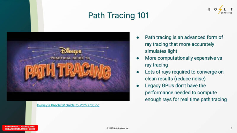
Bolt Graphics is trying to do Path Tracing in hardware.
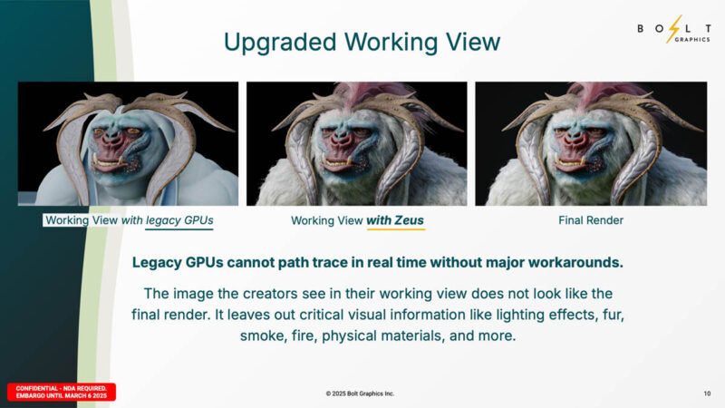
One of the benefits to having better hardware is that artists can see much closer representations of what final renderings will look like. If you have ever heard Pixar, or other studios discuss what they do, they generally have huge render farms that take a long time to render each frame accurately.
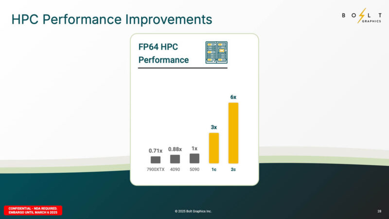
We will go into architectures later, but the 2.5x speedup for the 1c part is the single chiplet GPU with 400GbE and around 120W TDP apparently.
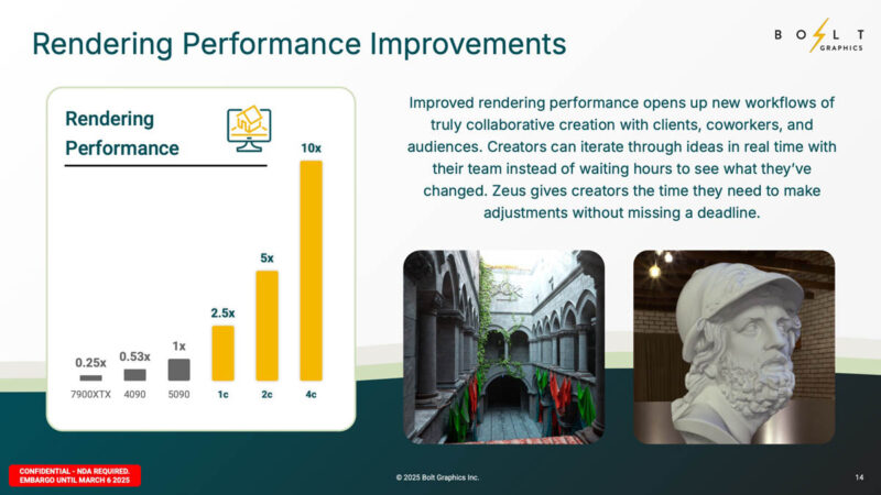
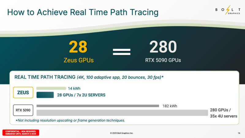
Of course, the idea is that you can scale the number of GPUs and get to higher performance levels. Something that is notable here is the comparison to the NVIDIA GeForce RTX 5090, not a NVIDIA RTX 6000 Ada, H200, or something similar.
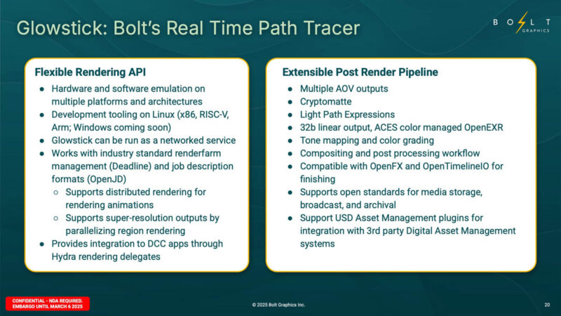
Bolt Graphics has a real time path tracer called Glowstick.
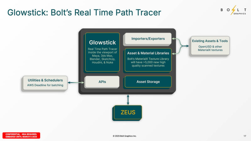
This may not be a completely fair statement, but in the world of GPUs, the software development and support side is a huge deal. Something like a path tracer is a specific area that Bolt could develop for customers.
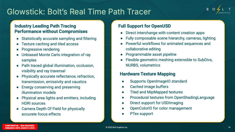
We are going to let folks read through the Glowstick features on these slides.
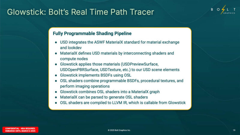
This is one of Bolt’s key features for customers.
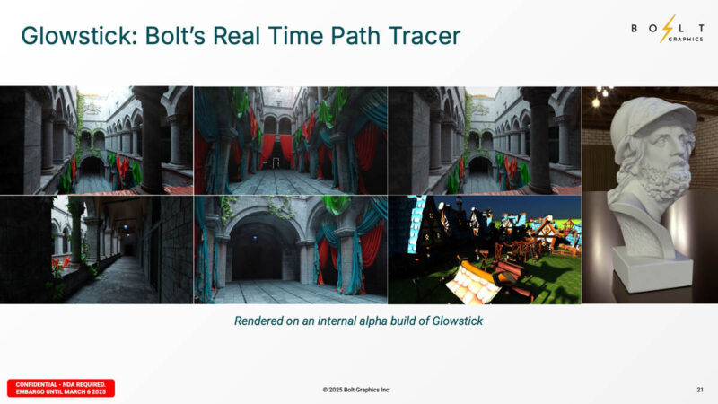
Here are some demo renders on an Alpha build of Glowstick.
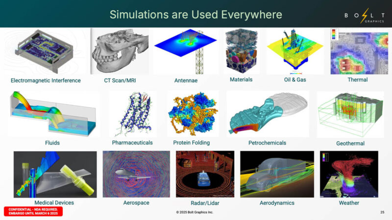
Another use case for Zeus is HPC simulations.
This FP64 performance slide we need to take into some context. NVIDIA years ago decided that FP64 was a data center GPU feature not a consumer GPU feature.
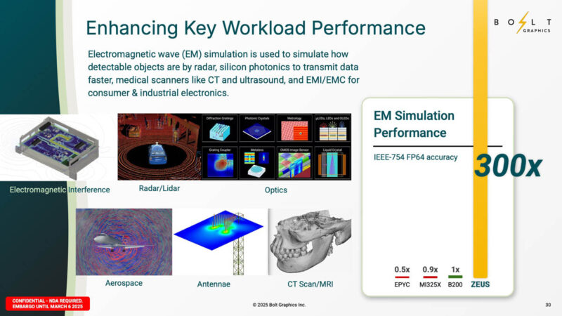
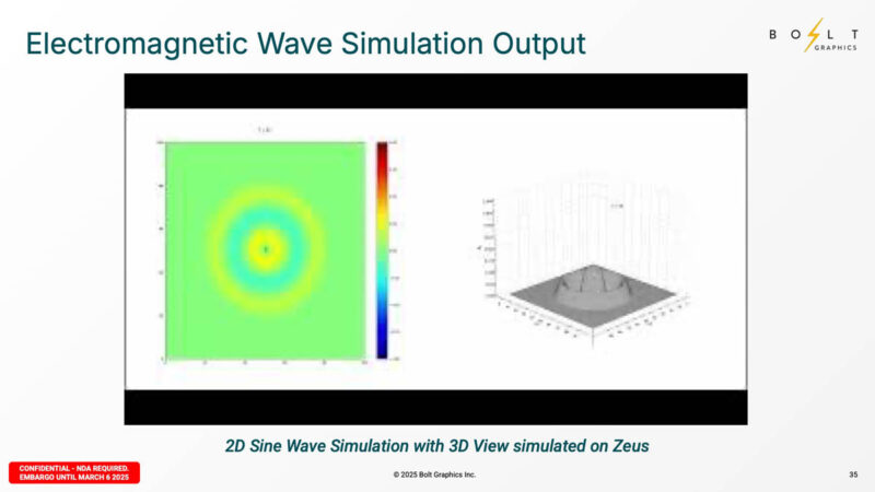
One application is electromagnetic wave simulation where Bolt is claiming Zeus is much faster.
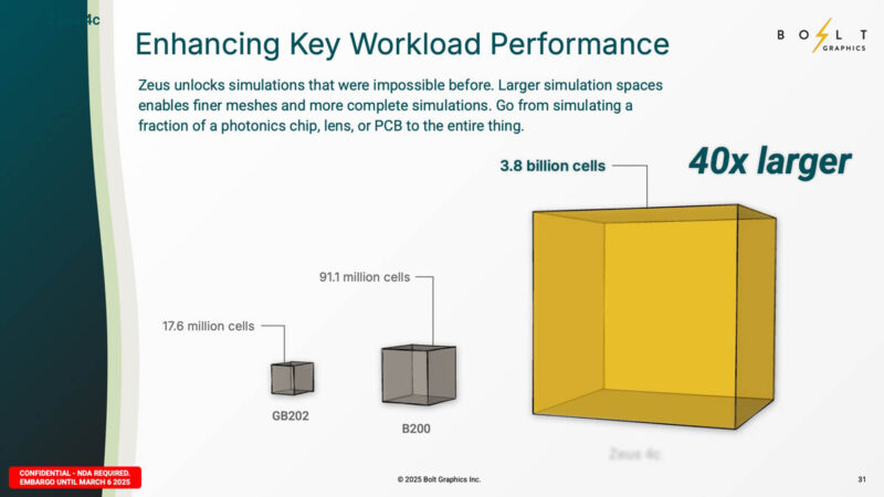
Aside from speed, Bolt is saying that it can handle larger simulation spaces, especially using the 4c model.
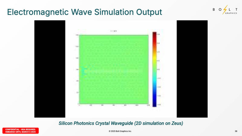
In the announcement deck, Bolt Graphics had a number of simulations.
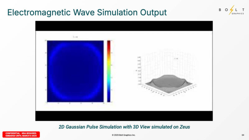
Here is another one.
And another.

Here is a FFT simulation. FFT simulations are a big area.

Here is a silicon photonics crystal waveguide simulation.
Here is another way to look at Zeus in the HPC space. Bolt Graphics has a focus on FP64 and FP32 compute and is looking to do things at a different performance, price, and capacity space than many of the GPUs today.
Next, let us get to the architecture.


The general sentiment is that if “Bolt graphics” had anything revolutionary, they would have been bought out by one of the major players.
They’ll be at Hot Chips, and maybe they’ll have something real to show by then. Lots of big promises and marketing fluff so far.
The marketing looks attractive to me in that they claim enough tflops and memory bandwidth to be interesting. From my point of view it’s not just cost-power-performance that’s important but the software stack.
In that direction RISC-V inside sounds similar to the cancelled Intel MIC approach. If it works, then it might be significantly easier to program than the weird instruction set architectures used by current GPU accelerators
You can bring a gpu back from two decades in the future but if the software compatibility isn’t better than the current state of AMD’s then it’s gonna be tough to grab any meaningful market share.
Matrox is still making GPUs…
I have one question we should all be asking ourselves right now.
If a small startup can deliver 2.25TB of memory, why does NVIDIA limit us to 24GB on consumer GPUs?
If I were Bolt Graphics, I would focus my resources on developing and fine-tuning LLM-assisted coding to rapidly build a comprehensive software ecosystem that competes with CUDA, TensorRT, PhysX, G-SYNC, and NVIDIA’s SDKs. Their hardware already proves that NVIDIA, AMD, and Intel have been artificially limiting advancements, releasing minor upgrades while creating a false sense of scarcity.
The industry constantly pushes the narrative that hardware is never enough, keeping demand high while restricting access to more powerful configurations. Zeus GPUs show that a small company can deliver what the big players refuse to release. If Bolt wants to succeed, they must break away from hardware-first thinking and aggressively build the software foundation that will drive adoption.
First impression is very positive one, at least for me.
They are so different that they don’t really need to directly compete with nVidia/AMD/Intel etc.
If their thing allows some interesting generality aspects that dGPU can’t touch due to its uniform “many stupid execution units goose-stepping oover every problem”, they have a winner.
Looking at the performance examples they’ve chosen to share it’s clear that there’s extreme cherry picking for examples that are purely mathematical. Combining this with the small memory bandwidth as per the specs it’s pretty clear that these GPUs will suffer for any tasks where larger amounts of data or load/store operations are required.
Another red flag is the hyperfocus on hardware and barely mentioning software side of things (like SDKs, compatibility with common frameworks and applications etc.)
Isn’t this basically just Xeon Phi, but with RISC-V instead of x86?
Just goes to show you that NVIDIA, a $2.71T company is actually a B.S company that rips us off if a small startup company can easily develop a GPU with 2.25TB of memory.
We need more players in this competition otherwise we will suffer financially and as can everybody see, NVIDIA love’s money more than their tech anyway.
Anyone remember Bitboys Oy?
“Anyone remember Bitboys Oy?”
They might not have released the promised hardware, but they did have valuable people and IP. First ATI bought them and then later, when AMD had bought ATI, they sold the IP (Imageon) and team to Qualcomm…
Why would Qualcomm want it? Because Adreno is based on the technology. Not such a failure as you remember, now is it?
Color me skeptical. RiscV has put many interesting benefits on the table, but performance has yet to be one of them and doing chiplets at this scale with it is all new. I also doubt they will be able to use slotted memory and be able to keep timings in check with the parallel complexity that comes with a GPU.
I wish them all the best because competition in this area is desperately needed, and I also appreciate they are not using the AI gimic to gather interest that will ultimately amount to nothing. Hopefully that bubble pops some before this comes to market.
@gyges3D: GDDR @ max. 2GB / chip and max. 2×12 chips / GPU = max. 48GB per GPU. For its consumer-grade cards, NVIDIA only offers one chip per bus. The big three DRAM manufacturers are expected to launch 3GB capacities with GDDR7. Theoretically, they could go higher but they would rather sell HBM in the AI data center space.
NVIDIA’s Project DIGITS platform will be its first to use the slower LPDDR, much like Bolt. Note that Apple just announced a configuration limit of 512GB for the Mac Studio with M3 Ultra, so either they have 64GB LPDDR chips now or that platform uses a hybrid LPDDR / DDR memory architecture, as Bolt does. Stay tuned for the teardowns.
IIRC Apple’s earlier Mx chips had their RAM inside of the SoC, so tearing an M3 Ultra down may not tell anyone a whole lot. IIRC they’re claiming >800 GB/sec of memory bandwidth, which would be a *lot* of pins if they carried that externally.
Wikipedia says the M3 Max uses LPDDR5 6400, so there are presumably 16 channels under the hood to get 800 GB/sec, assuming they’re not cheating and the M3 Ultra is really 2x Maxes as advertised. That’d be 16x 32GB chips, right?
Is it known if it’ll use ECC RAM? Anything known about pricing?
@Scott Laird: Apple buys the LPDDR chips and includes them in its SOC packages, so you can clearly see them immediately adjacent to the central die after the joint heat sink is removed. Also, Apple uses 128 bit memory bus controllers and one chip per controller. 8 buses * 128 bits / bus * 6400 Gbit/s * 1 byte / 8 bits = 819,2 GB/s.
Until now, the capacity limit was 32GB / chip but Apple is now offering up to 512GB on the Mac Studio. So either they have sourced 64GB chips or they have changed their memory architecture.
This article would benefit from adding the tag: RISC-V
This CPU reminds me of STH’s article about “Ventana Veyron V2 RISC-V CPU Launched for the DSA Future”, but less.
@gyges3d March 6, 2025 At 10:21 pm
“I have one question we should all be asking ourselves right now.”
Watson Jr. memo about CDC 6600 ;-)
https://www.computerhistory.org/revolution/supercomputers/10/33/62
Anything in the GPU market sphere is welcomed. The more competition the better. I’ve had enough of the Ndiva dominance and pricing.