ASUS RS700A-E13-RS12U
For more standard compute servers, we have the 1U ASUS RS700A-E13-RS12U. In the front, there are 12x 2.5″ NVMe drive bays. Front NVMe balance with CPU TDP is a challenge in 1U servers, and here, ASUS is optimizing storage density.
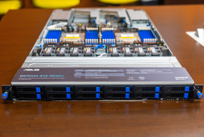
This server sports dual AMD EPYC 9005 CPUs, up to 300W TDP each.
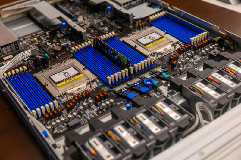
There is also a dual M.2 module in the middle and 24 DIMM slots total.
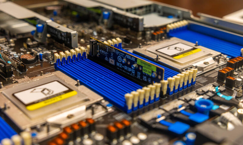
The motherboard has a very modern design with MCIO x16 riser slots, MCIO front connectors, and OCP NIC 3.0 slots.
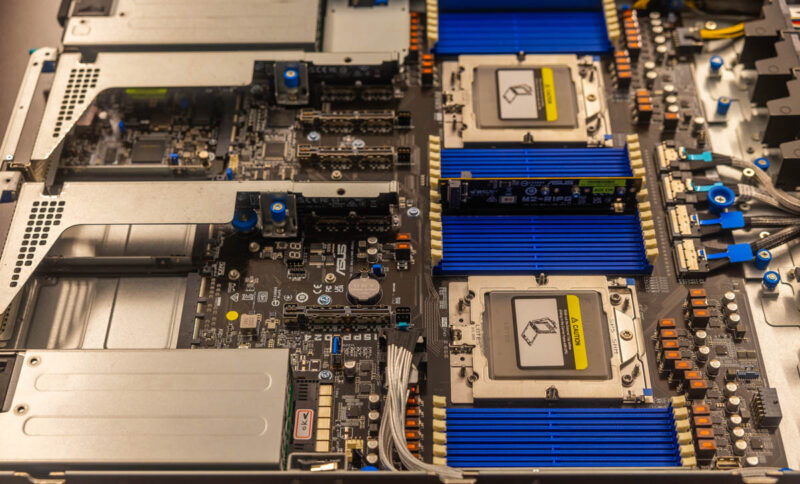
Here is a quick look at the risers.
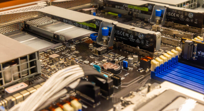
In the rear, we have a management port and two OCP NIC 3.0 slots plus two full-height PCIe Gen5 x16 slots.
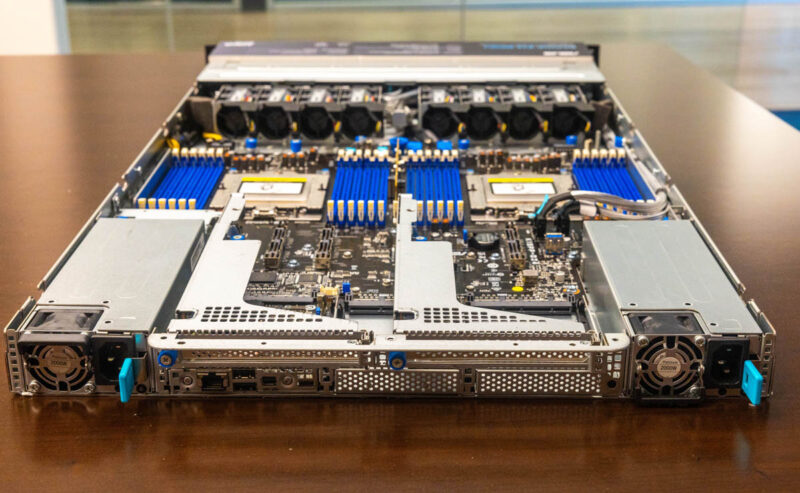
This is a more standard 1U dual CPU design, but it is packed with functionality.
Final Words
These are some neat new systems. Still, the standout to our team was the ASUS RS520QA-E13-RS8U. The 2U 4-node single socket AMD EPYC 9005 was interesting, especially since even at a single socket, it scales to 192 cores. The big one, however, was the CXL expansion, which gives a straightforward path to adding even more DIMMs to each node. That is just so different that it is really neat.
Thank you to ASUS for letting us stop by and see some servers that were both on the OCP Summit 2024 show floor, but also at their offices.


On the CXL system; is there any sort of inter-node connection to allow flexible allocation of the additional RAM; or is it purely a measure to allow more DIMMs than the width limits of a 2U4N and the trace length limits of the primary memory buss would ordinarily permit?
I’d assume that the latter is vastly simpler and more widely compatible; but a lot of the CXL announcements one sees emphasize the potential of some degree of disaggregation/flexible allocation of RAM to nodes; and it is presumably easier to get 4 of your own motherboards talking to one another than it is to be ready for some sort of SAN-for-RAM style thing with mature multi-vendor interoperability and established standards for administration.
It is not obvious where the other four GPUs fit into the ASUS ESC8000A E13P. Is it a two level system with another four down below, or is ASUS shining us a bit with an eight-slot single slot spacing board and calling that eight GPUs?
Oh, nevermind. Trick of perspective, the big black heatsink looks like it would block any more slots.
Page 1 “The 2.5″ bays take up a lot of the rear panel”
I think you mean “The 2.5″ bays take up a lot of the **front** panel”
Hard to imagine telling us any less about the cxl! What’s the topology? Can the cxl RAM be used by any of the 4 nodes, and how do they arbitrate? What’s the bandwidth and latency?