

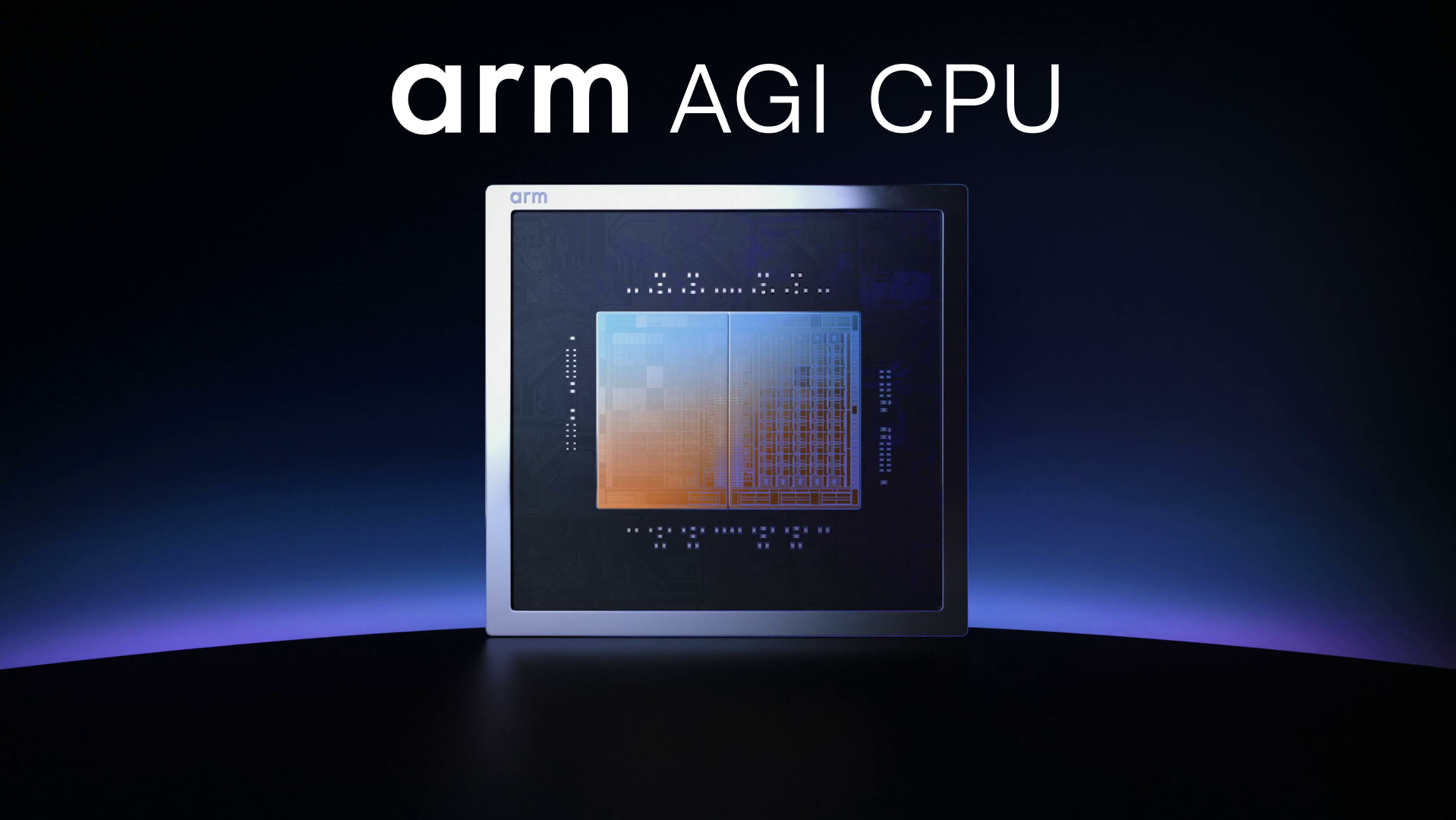
Continuing with our coverage of the second CPU session of the day for Hot Chips 2026, we have Arm’s presentation. The long-time chip IP designer is at the conference to talk about their very first complete commercial CPU design, the AGI, which is aimed at the AI and data center market. Based around the latest and greatest of Arm’s CPU IP, not the least of which is the Neoverse V3 CPU cores, Arm is breaking new ground by offering their own CPU directly to server vendors rather than just selling the IP. It is a significant change of pace for the company, and one that lets them control their own destiny like never before.
Please note, we are covering this live, so please excuse typos.
Arm’s AGI Data Center CPU at Hot Chips 2026
Though this is Arm’s first in-house CPU, the company is no stranger to CPU design. The Neoverse V architecture family is now on its third generation, after the Neoverse V2 powered a large number of CPU designs both for commercial chips and chips used internally at the major hyperscalers. AGI, in turn, is designed to be a tour de force of Arm technologies, adding up to a powerful chip that is meant to drive the next generation of agentic AI servers, with up to 136 V3 cores per chip.
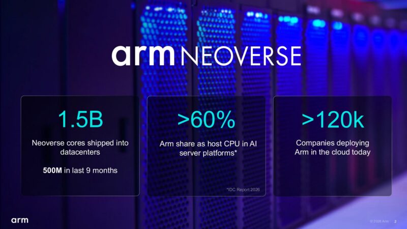
Many companies are using Arm Neoverse these days.
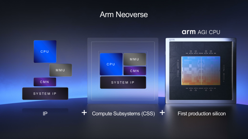
AGI has been a journey for Arm. Over the years they have gone from designing IP, to designing entire compute subsystems (CSS) blocks, to now their first in-house commercial chip.
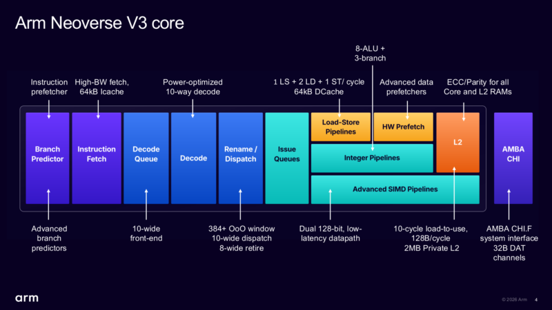
The Neoverse V3 core is designed for a balance between performance and power efficiency. That meant hitting a minimum performance target for a single core. The V3 core has a private 2MB L2 cache, and a 128-bit SVE2 SIMD.
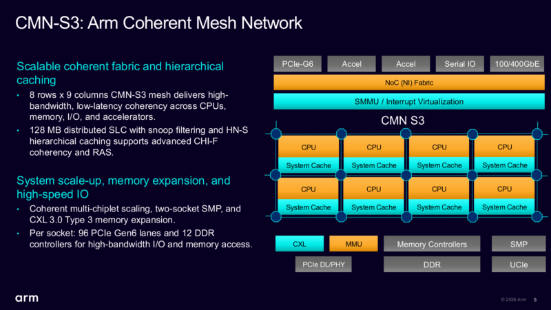
The CMN-S3 mesh needs to meet multiple goals for Arm. It needs to scale across a lot of CPU cores, and able to carry a lot of memory bandwidth. As well, it needs to carry an extensive amount of I/O bandwidth for PCIe devices and such.
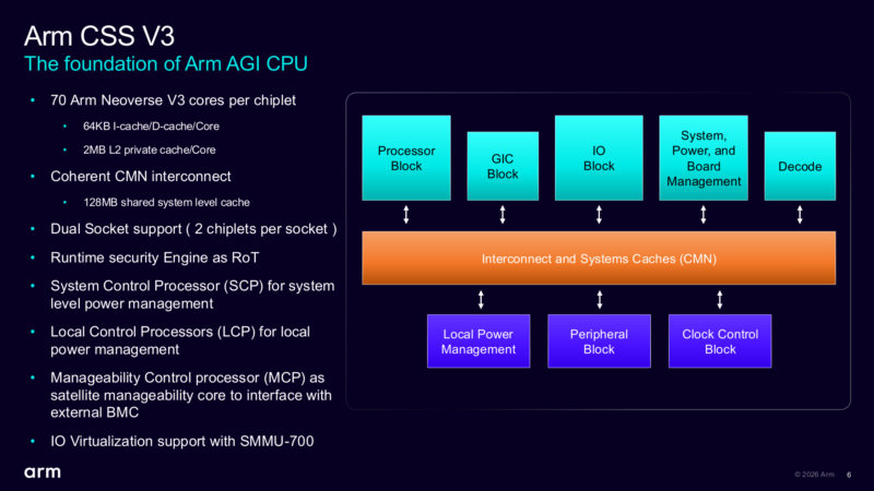
AGI is built from Arm’s Neoverse V3 CSS. There are 70 CPU cores per chiplet, attached via the CMN fabric.
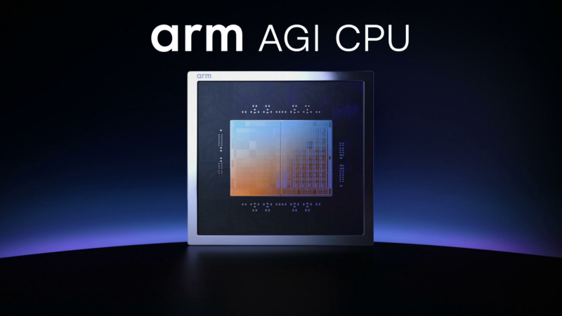
SoC design is an optimization around the physical limitations of the platform. This drove Arm to use chiplets, with a pair of chiplets making up a single AGI chip.
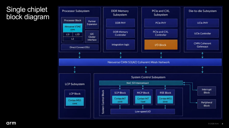
Looking at a single chiplet, there 35 compute tiles in each chiplet. This is joined with a DDR memory subsystem as well as an I/O subsystem for PCIe and CXL devices (as well as connecting to another socket). There is also a dedicated D2D subsystem to connect to the other chiplet. It runs at 32Gbps/lane, which is an incredibly high data rate, and is designed to ensure the D2D connection is not a bottleneck, and that the chip comes very close to functioning as a single monolithic chip.
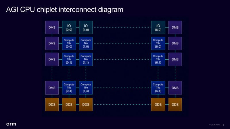
Each tile has 2 CPU cores, with the tiles existing in a mesh that balances the CPU cores with the memory, IO, and die-to-die subsystems.
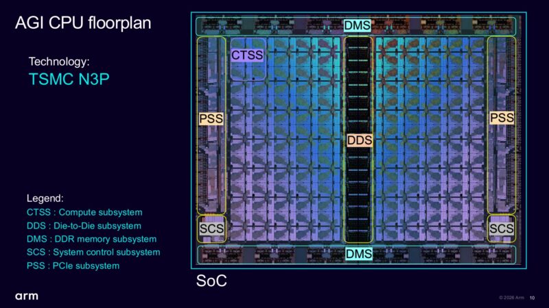
Looking at the actual floorplan (note that this is rotated compared to the logical diagram).
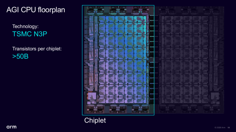
Arm opted for TSMC N3P for the AGI chiplets. The company picked N3P because it is a performance and proven process node, the undertext being that Arm didn’t want to take a chance on (or didn’t have access to) an N2 node at this time. There are more than 50 billion transistors per chiplet.
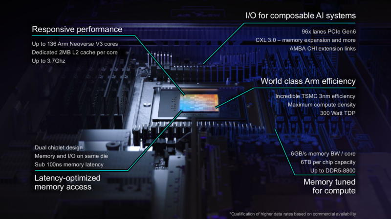
Each SoC can support up to 136 Neoverse V3 cores. There are 144 cores in hardware, but the remaining core are for die harvesting purposes. Each CPU core can run at 3.7GHz; Arm didn’t spend the gates or die area for higher frequencies as they wanted to maximize energy efficiency.
The aggregate memory throughput is over 800GB/second, which works out to around 6GB/second per core.
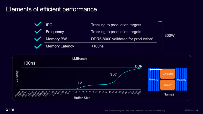
All of this is on a 300 Watt TDP. IPC and frequency is at their production goals. And memory latencies are low in a NUMA 2 configuration.
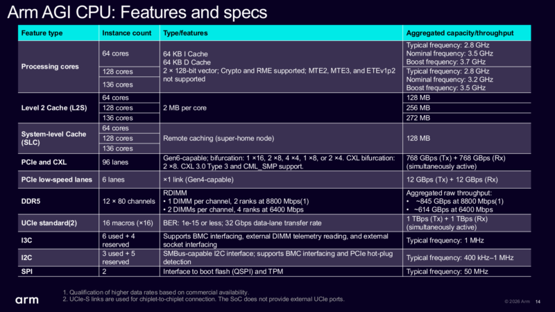
Looking a bit more at the specs, the 64 core parts will be allowed to run at slightly higher frequencies, boosting as high as 3.7GHz with a nominal frequency of 3.5GHz. Meanwhile the higher core count chips are running at a nominal 3.2GHz with a max boost clock of 3.5GHz.
Meanwhile, a 12 channel DDR5 memory system allows for 845GB/second of bandwidth using DDR5-8800. It can hit those speeds at 1DPC, while 2DPC drops to DDR5-6400 speeds.
Arm intends to match I/O bandwidth to memory bandwidth in their designs.
Arm is also using UCIe for their D2D subsystem, with two x16 modules. That allows for 1TB of bandwidth in each direction between the dies, and means there is more D2D bandwidth than memory bandwidth, in order to keep NUMA-1 mode performance high.
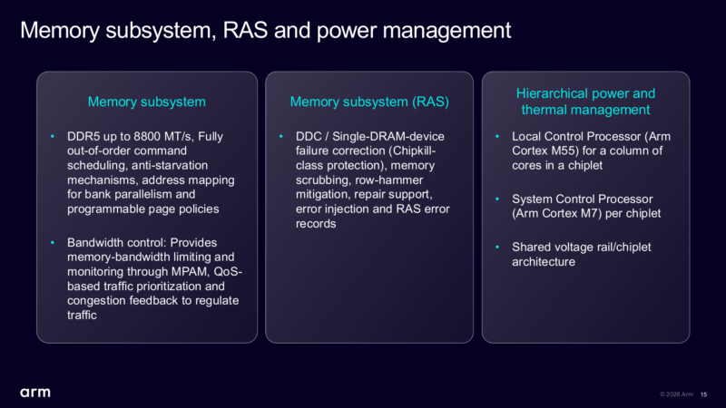
Diving a bit deeper, here is AGI’s memory subsystem. Arm uses MPAM resource partitioning to help ensure consistent performance of the chip as well as reducing starvation. The hardware also supports programmable page policies.
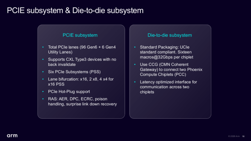
The six IO subsystems allow for a total of 96 PCIe Gen6 lanes as well as another 6 Gen4 lanes for utility purposes. The hardware supports bifurcation down to 4×4. Customers can also use CXL 3.0 here (including Type3 devices) for more advanced hardware.
Meanwhile the D2D subsystem uses UCIe, 16 lanes at 32Gbps each.
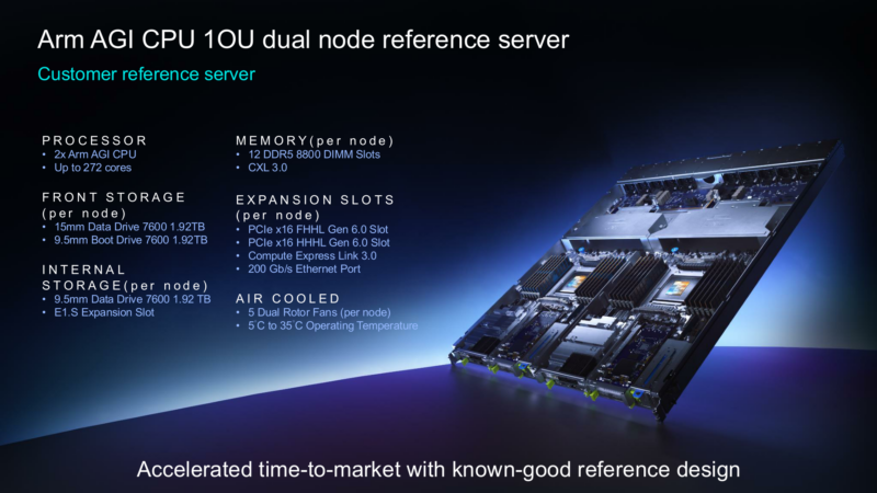
Here is a quick look at Arm’s reference server.
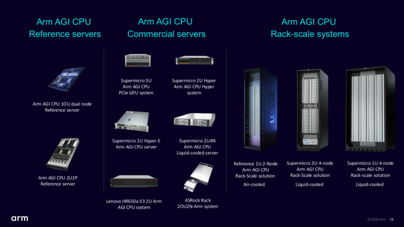
But there will be multiple vendor designs to cover many different use cases. Everything from rack-scale systems down to more traditional commercial servers.
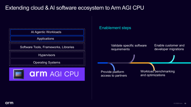
And while not a focus of this presentation, software plays a huge role in the overall ecosystem.
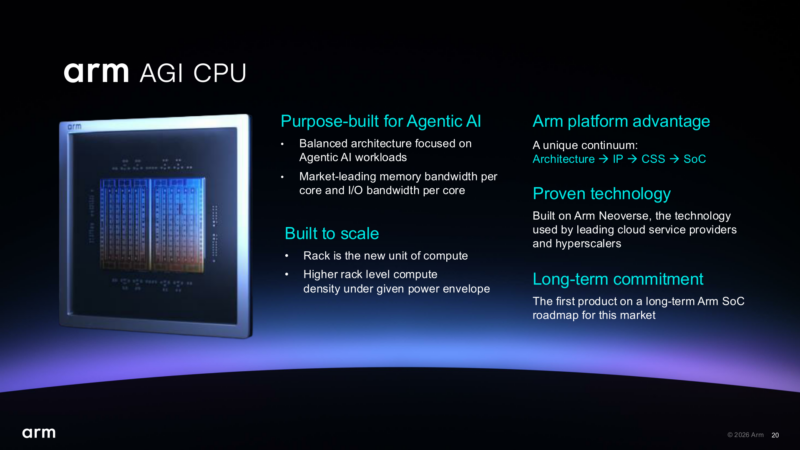
Wrapping things up, AGI is the first part of a long-term hardware commitment for Arm. The company has an extensive SoC roadmap for future generations of data center processors, underscoring their commitment to producing their own chip for the server market.
We have a full recap on the Substack, including where all of these pieces ranked in terms of popularity:


I am not understanding why they are still on Neoverse V3 CPU which is design from 2024, but based on design from their Laptop / Smartphone in 2023.