AMD Instinct MI300 Packaging Technologies
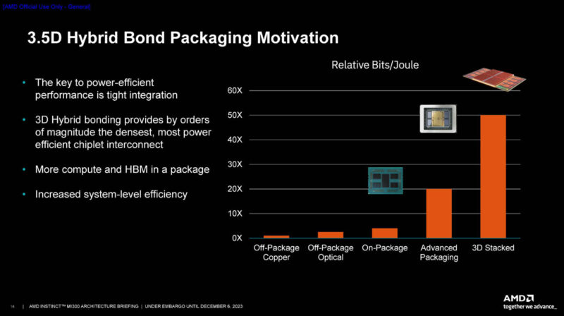
AMD calls this the 3.5D hybrid bond packaging technology. A big part of the new technology is co-packaging memory and compute to lower the energy used to shuttle data around the chip and system.
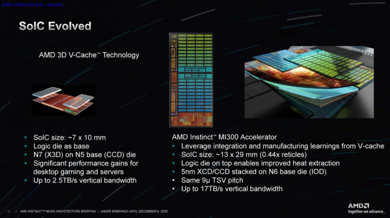
AMD is using a 7nm 3D V-Cache tile with a base 5nm CCD. AMD says that having millions of consumer and server chips with 3D V-Cache makes this much easier to integrate.
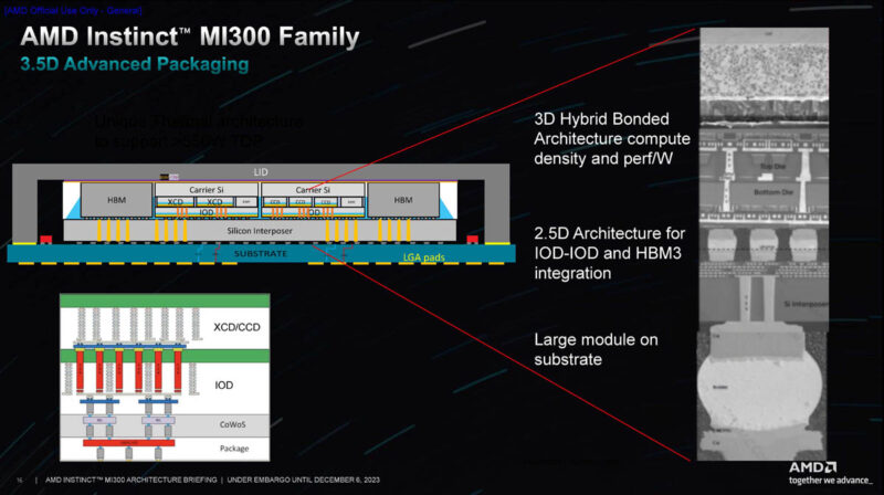
Here is the die stack. AMD has HBM and the IO die on the silicon interposer and then is using 3D hybrid bonding to achieve higher density. This is a few steps beyond what NVIDIA is doing on the H100, H200, and GH200 parts.
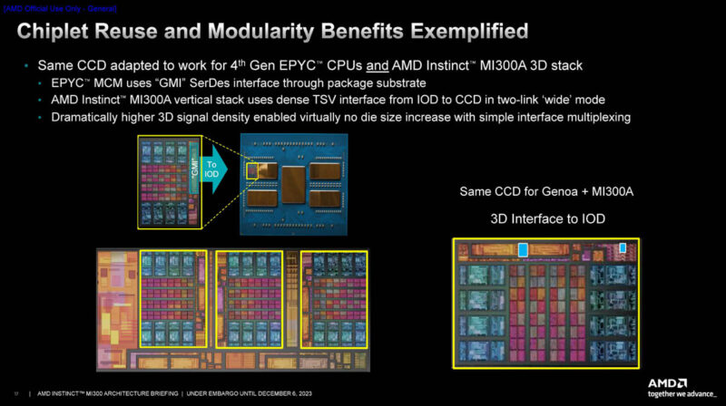
One of the key enablers is that AMD is using CCDs, IO Dies, and more from other products and with small tweaks is able to use them on the MI300 family. A few months ago I told Forrest Norrod at AMD that I felt like his chiplet strategy was to make a few chiplets and options and then just mix and match to make targeted chips for different applications. He did not necessarily disagree with me.
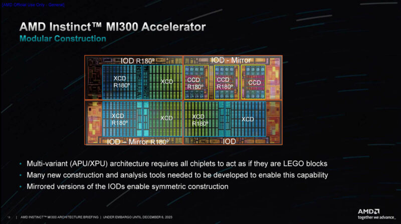
Here is the layout without the HBM3 on the edges. One of the challenges was to do things like create the vertical wires in the IOD to stack the XCD and CCDs. Something that is also notable here is that there are these R180 and Mirror blocks. These are where AMD has rotated the dies and is using a mirrored version to get the rectangle geometries to work.
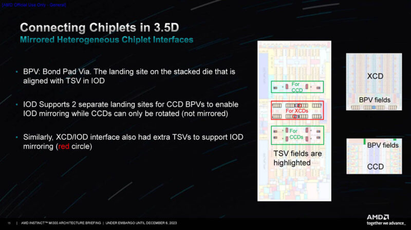
BPV or Bond Pad Via and TSVs were important for getting this to all work. AMD went into a lot of detail around how it had to work with teams on different projects to ensure that the IP it was building, such as the IOD could be leveraged for server CPUs as well as for the MI300 family.
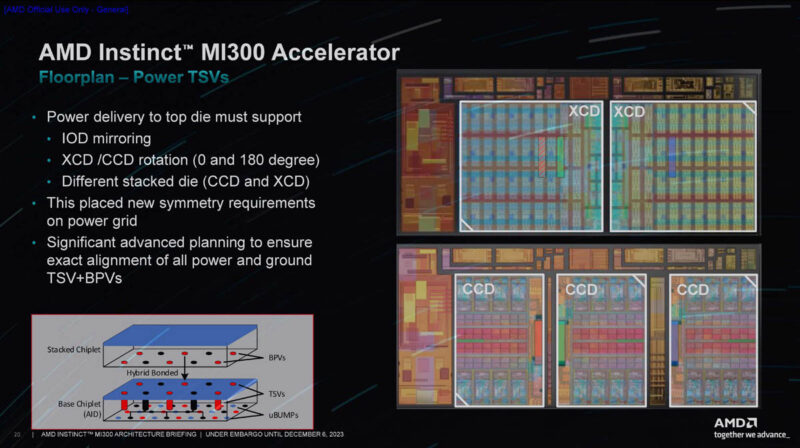
Here is a quick floorplan with the MI300A.
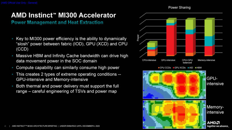
Another big feature of having the MI300A APU is that it can share power with critical parts of the package during different types of applications. Different applications can stress memory more or GPUs more. AMD had to model these and figure out how to power and cool the large package. Folks know how to model and deal with chips like Genoa today. This 3.5D stacked package is cutting edge for a production part, with perhaps only Intel Ponte Vecchio being more complex.
A lot had to go into the packaging to make this all work.
AMD ROCm 6 and AI Software Support
AMD has a lot of AI software stacks from ROCm for the GPU. ZenDNN for inference on its CPUs, and Vitis AI for things like Xilinx Kria KV260 FPGA-based Video AI Development Kit.
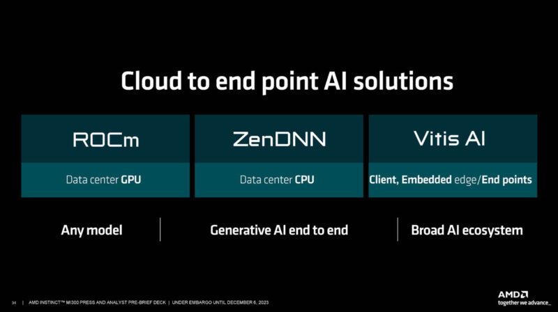
ROCm is really the key to get the MI300 to stick with customers since that is the primary stack for the MI300X and MI300A. Most users may interact with higher-level frameworks, but those frameworks need to work (well) with the hardware. NVIDIA spends a ton of money on CUDA.
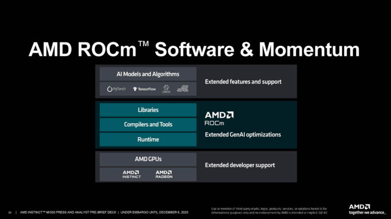
We now have ROCm 6. This is the next-generation and more AI-focused ROCm. It is easy to forget at an AI event, that ROCm was launched with a focus on HPC.

AMD is touting ROCm 6’s optimizations for AI applications.
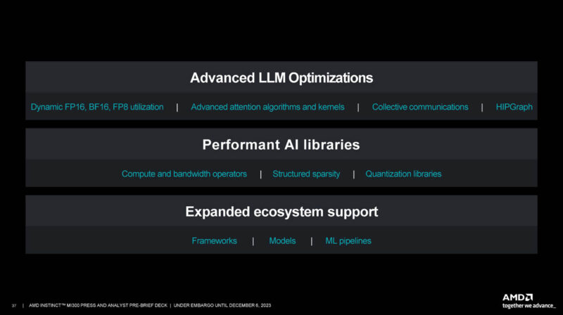
One part of the equation on using GPUs for AI is getting them to just work. We have heard this is mostly fixed at this point. The next is having competitive hardware. AMD is certainly competitive in memory and compute. Finally, software is often where the big gains happen. NVIDIA gets a lot more performance out of its hardware over time through optimizations.
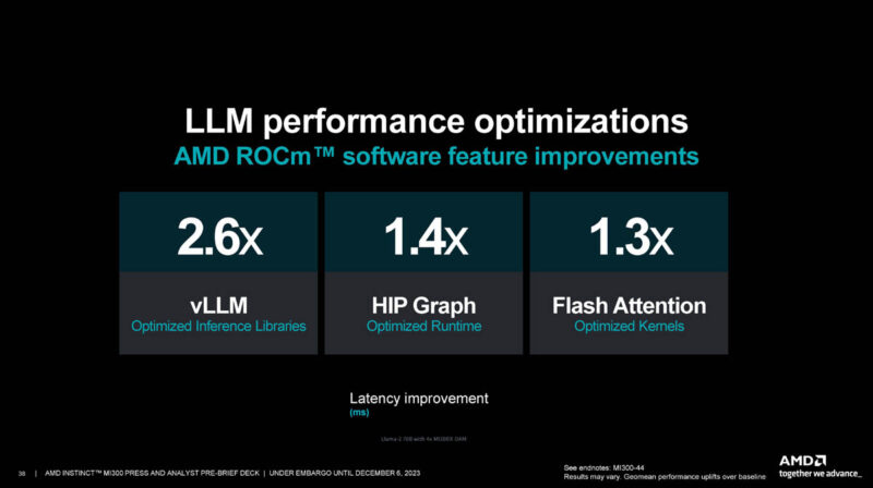
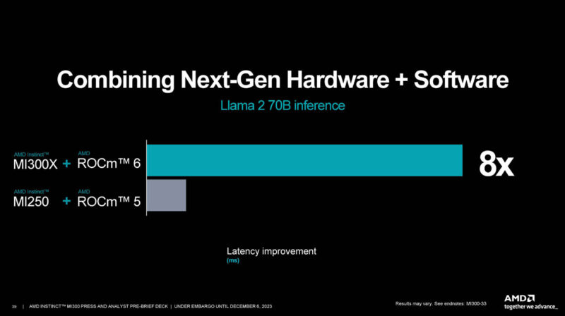
AMD talked about the hardware plus software gains and says it can see 8x performance gains.
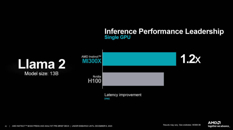
Here is another AMD versus NVIDIA single GPU inference.
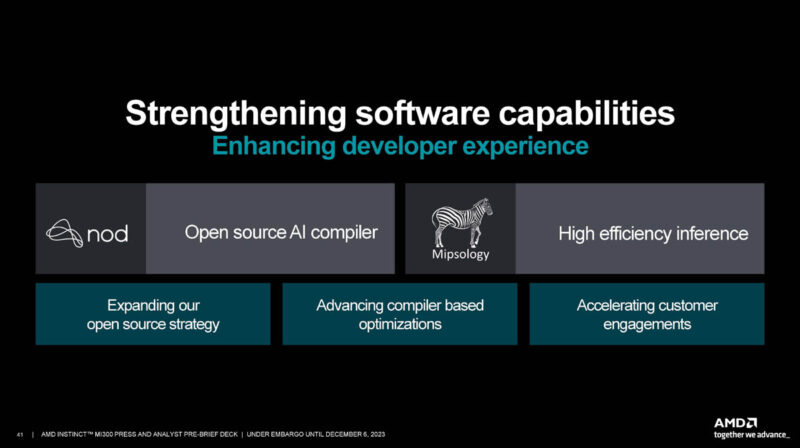
AMD purchased Nod and Mipsology to help its software stack.
It also is touting that it has integration with popular frameworks.
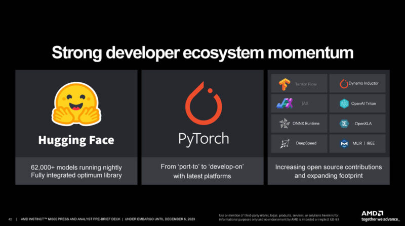
The basic message on the software side is that AMD works. The open question is about scaling and optimizations over time.
Next, let us at least show the end notes. Then on the next page wrap this up.
AMD End Notes
We also wanted to publish the end notes for the presentation since there are a lot of performance claims.
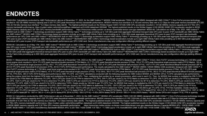
Here is another page.
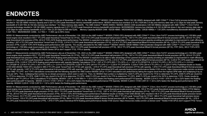
Lots of small text here.
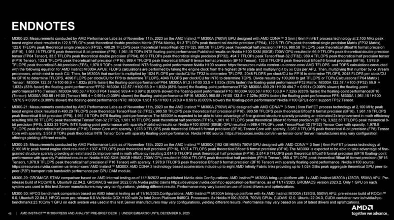
Here is another set of endnotes.
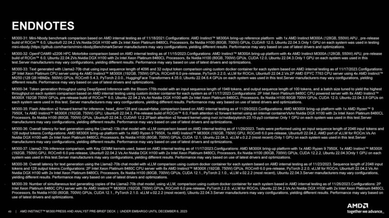
Here is yet another.
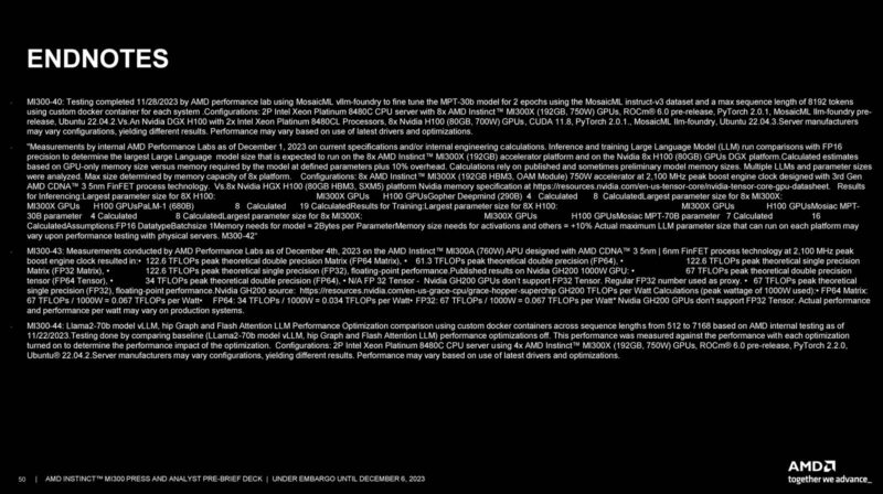
That may not be the most exciting, but we at least wanted to have these documented.
Next, let us get to our impact discussion.

STH testing when?
Great article as always Patrick and Team STH
It looks like a couple of MI300A systems are available: https://www.gigabyte.com/Enterprise/GPU-Server/G383-R80-rev-AAM1 and https://www.amax.com/ai-optimized-solutions/acelemax-dgs-214a/
Couldn’t find prices but if it’s supposed to compete with GH then it’ll be around U$30K.
It’s a good question which of the MI300A or MI300X is going to be more popular. As a GPU could the MI300X be paired with Intel or even IBM Power CPUs?
I personally find the APU more interesting. Not because the design is new so much as the fact that real problems are often solved using a mixture of algorithms some of which work well on GPUs and others better suited to CPUs.
Do you know if mi300A supports CXL memory?
I hope to see some uniprocessor MI300A systems hit the market. As of today only quad and octo.
Maybe a sort of cube form factor, PSU on the bottom, then mobo and gigantic cooler on the top. A SOC compute monster.
In the spirit of all the small Ryzen 7940hs tiny desktops. Just, you know, more.