With the launch of AMD EPYC we can finally go into detail about the AMD architecture codenamed “Naples.” CPU design is extremely dense. The vast majority of people who use and purchase servers have very little need to know exactly how each architecture works. Likewise, those who use servers often just want to know will it work out of the box or will it be painful requiring hand compiling every bit of code at every turn.
When we set out to do the AMD EPYC architecture piece as part of our launch content series, we realized that there are very few folks who can follow (or frankly care) about the intricacies of architecture. Still, the server market has largely been in a single architecture world for 5+ years after the Intel Xeon E5 series was first launched in Q1 2012. With AMD EPYC there is now an alternative in the market that will run virtually every piece of software out of the box. At the same time, it is a fairly radical design departure from what Intel offers in its generational cadence so we wanted to present an architectural overview for those who did not specialize in computer engineering or electrical engineering.
In this piece, we are going to focus on the cores and interconnects. We have another piece on the platform-level features of the AMD EPYC 7000 series. Both aspects have a significant impact on the value and having hands-on experience with EPYC in the data center we have unique insights we can share.
Introducing AMD EPYC 7000 Series ZEN Architecture
The AMD EPYC 7000 series is based on the same basic ZEN microarchitecture we saw with Ryzen. We are going to have a quick recap of Zen before moving into details of the server features. Here is the overview of the microarchitecture:
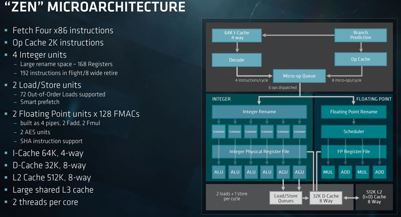
Each core is capable of handling two threads per core. We have seen architectures such as POWER and Cavium ThunderX2 go beyond two cores per thread in the space recently. Mainstream Intel servers are also two threads per core in a feature they call Hyper-Threading. AMD uses SMT and you can conceptually think of SMT and HT as similar features.
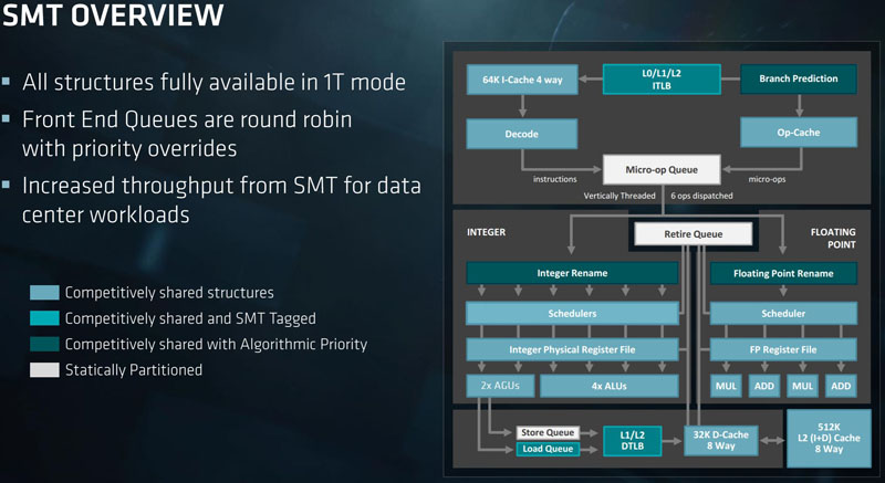
Beyond the basic core architecture, CPUs are made up of CCX complexes. CCX complexes are (up to) our cores with L1, L2 and L3 caches all interconnected. The best performance on AMD’s architecture is when workloads fit into these CCX complexes.
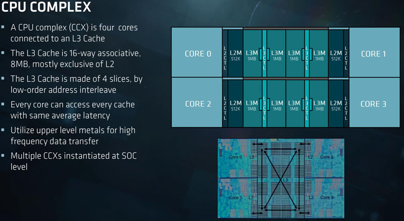
Although AMD says four cores on its slide, if there are less than 8 cores per physical die on a chip (e.g. the 8, 16 and 24 core EPYC 7000 series models and the Ryzen 3/ 5 series) some of these cores and potentially caches are disabled.
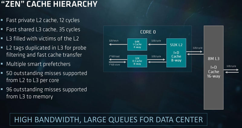
On the caches, AMD’s design has a 512KB L2 cache per core with an 8MB L3 cache per CCX complex. That adds up to be a lot of cache on a die which AMD’s architecture requires.
Here is an 8 core die shot of the AMD Ryzen chip with its two CCX complexes (left and right blocks you can see):
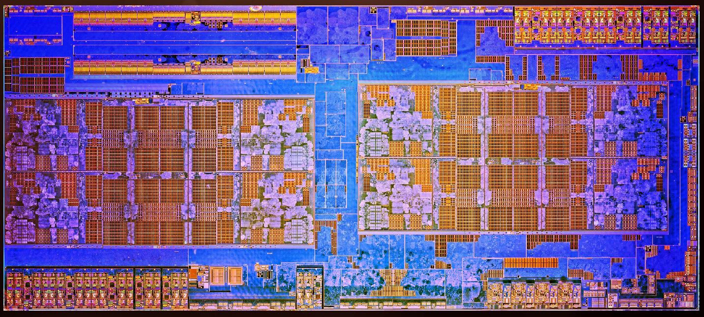
That gives each die up to 8 cores and 16 threads with 4MB L2 cache and 16MB L3 cache. AMD then takes these (up to 8 core) building blocks and puts four onto a package.
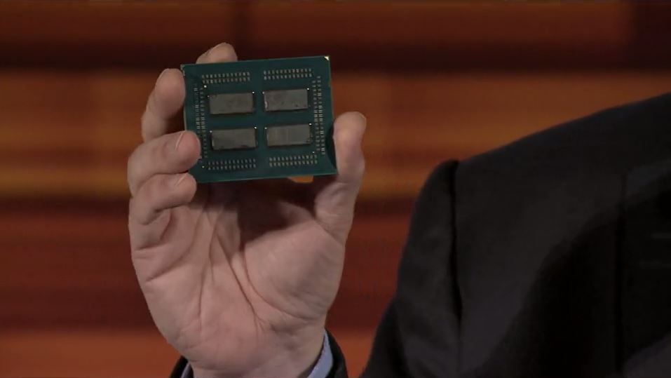
Using four small die per package allows AMD to keep manufacturing costs low while also delivering 32 cores / 64 threads, 16MB L2 cache and 64MB L3 cache per socket. Each die also has a dual-channel memory controller capable of 2 DPC operation. Unlike the desktop parts, each die can handle 128GB LRDIMMs and so with 16x 128GB per socket that yields 2TB per socket or 4TB of RAM in a dual-socket design.
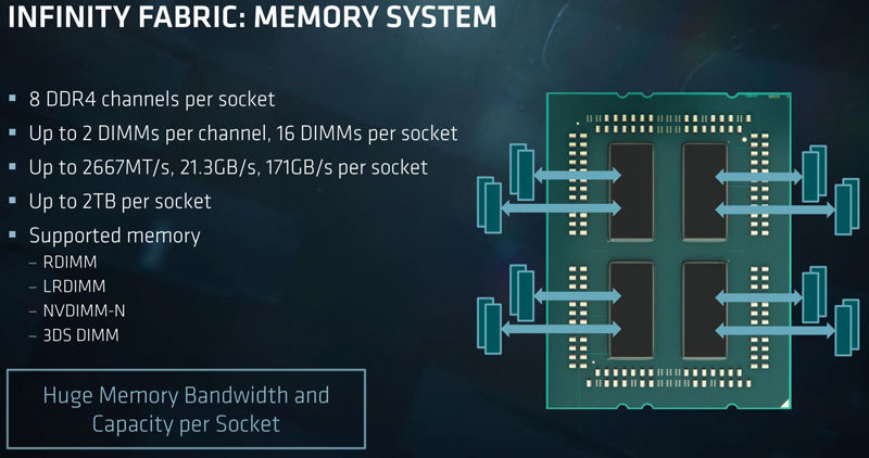
That design also means that there are four NUMA nodes per socket or eight NUMA nodes in a dual socket system. You can see this in Linux (here is a Ubuntu 17.04 lscpu output):

You can likewise see the 8 NUMA nodes in Windows:
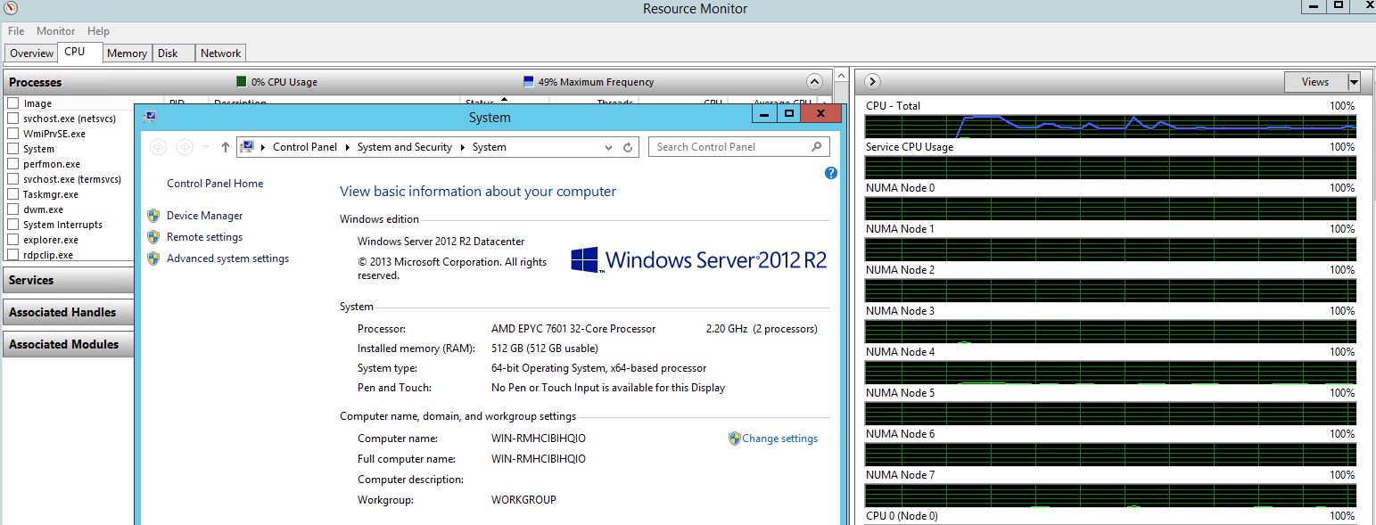
What that essentially means is that there will be different memory latencies depending on which die needs data from memory that can be attached to that die or another die on the fabric.
The AMD EPYC Infinity Fabric
To manage this complexity and move data around to each piece of silicon, AMD uses its Infinity Fabric. On a specific package, each of the four die had direct Infinity Fabric connections to each of the other die:
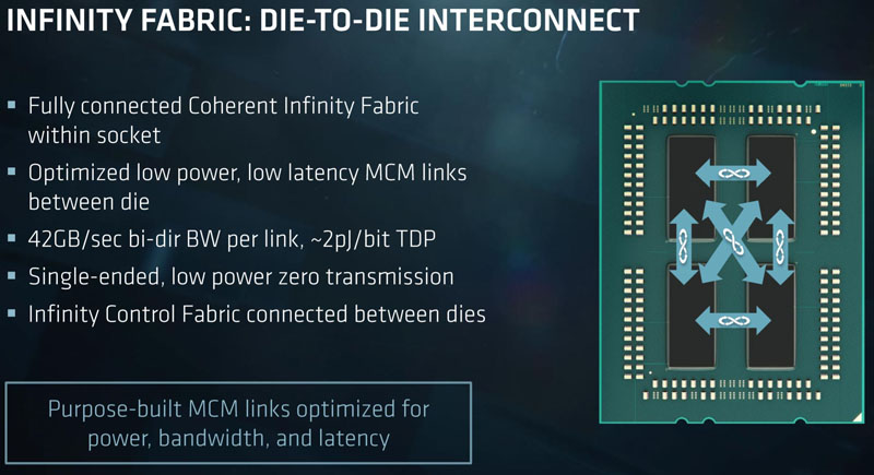
If you want to contrast this with Intel’s current ring architecture and next-gen Skylake-SP mesh architecture, we have a piece on that. The key difference is that AMD needs to go off die within the same socket where Intel stays on a single piece of silicon.
Moving to a socket-to-socket view, each die peers with a die on a second socket.
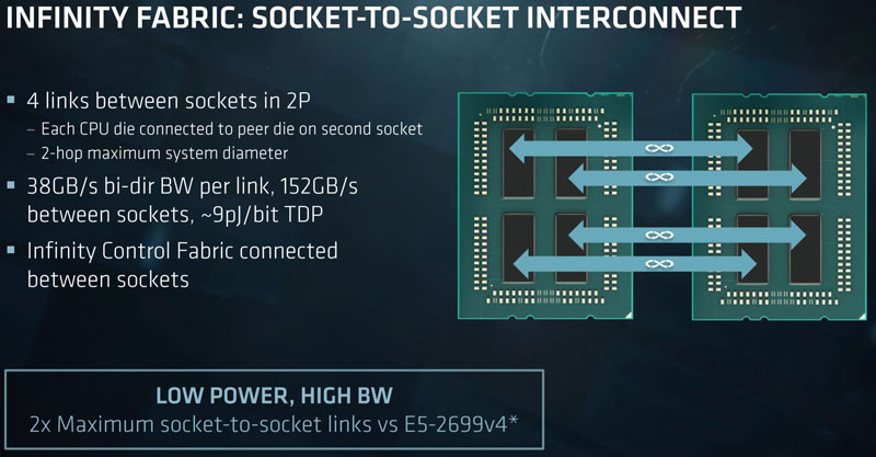
Practically while this means Socket 0 Core 0 can communicate in one hop to Socket 0 Core 3, communicating with Socket 1 Core 3 will require two hops on the fabric.
In terms of raw fabric bandwidth, here is what AMD presents as bandwidth features.
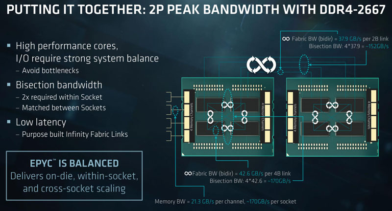
There are a few major caveats here. First, this fabric scales with memory speed. If you are using DDR4-2400 or DDR4-2133 you will have a fabric speed impact which is significant with 8x NUMA nodes on a dual socket system. Second, this die to die Infinity Fabric is carrying everything. PCIe-to-PCIe, DRAM, SATA storage, L3 cache data.
Infinity Fabric is a feat of engineering in itself. It helps AMD dramatically lower manufacturing costs. On the other hand, it does mean that there are significant performance variations as you move off die and onto the fabric. This is an area we will explore more fully in the near future.
More AMD EPYC Launch Day Coverage From STH
- AMD EPYC 7000 Series Platform-Level Features PCIe and Storage
- AMD EPYC 7000 Series Key Security Virtualization and Performance Features
- AMD EPYC 7000 Series SKU Lists for Launch
- AMD EPYC 7601 Dual Socket Early Power Consumption Observations
We will have more information on AMD EPYC as soon as we can release it.

