AMD has a new FPGA and hardened function NIC that it is presenting at Hot Chips 34. The AMD 400G Adaptive Exotic SmartNIC Architecture shown at HC34 has programmable logic, a hardnened NIC, and a 12-core Arm system. Let us get to it, but first, let us discuss what AMD is actually presenting. This is not the next Pensando part.
Note: We are doing this piece live at HC34 during the presentation so please excuse typos.
AMD 400G Adaptive Exotic SmartNIC Architectural Inflection Point
AMD decided to call this a “SmartNIC”. Since terms were used inconsistently, we created the STH NIC Continuum framework that has been used by not only STH (we are probably the primary industry coverage point for this class of device) and we have let several industry analysts use the framework.
In our framework, this is considered an “Exotic” NIC like the Intel IPU that we looked at in This Changes Networking Intel IPU Hands-on with Big Spring Canyon. Indeed, AMD even uses the use case we showed with Intel below as one of the use cases for its Adaptive Exotic Smart NIC.
The reason behind devices like this is that it allows one card to run in multiple customer data centers. Xilinx sells a lot to China, and that is a geography often with different cipher needs than in the US and Europe. As a result, having a FPGA allows a device to be flexible enough to address not just different use cases but also different customers.
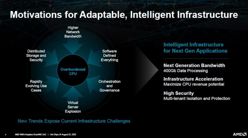
AMD recognizes this and there are a number of different customers for this type of device.
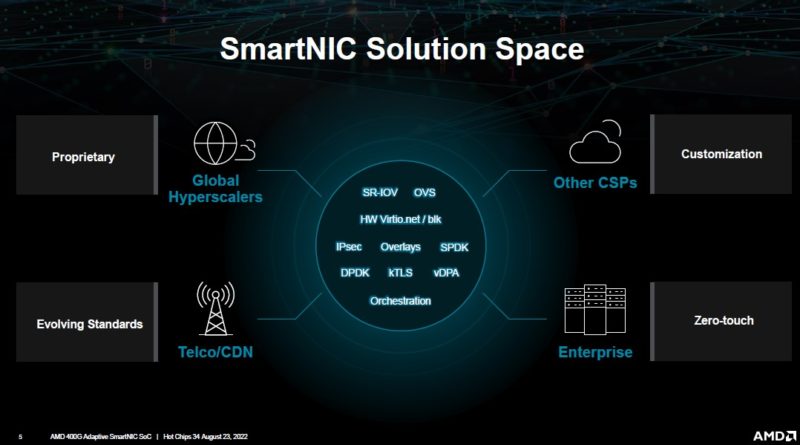
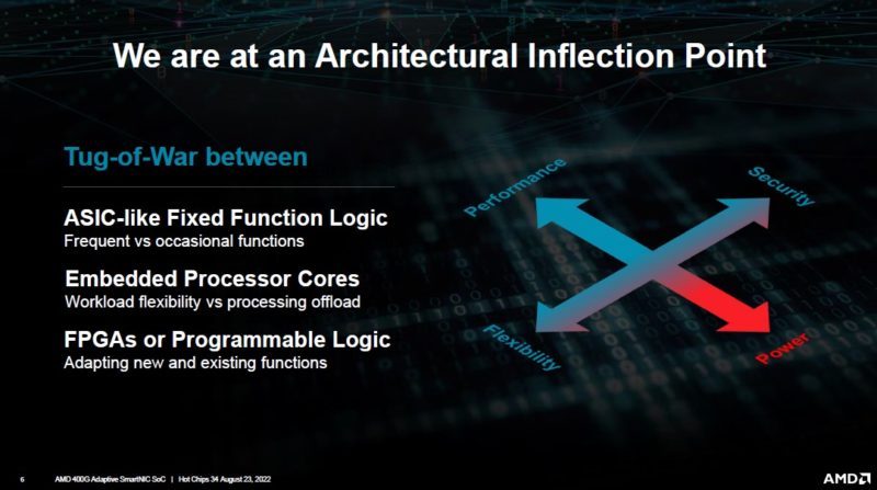
Instead of playing tug-of-war between architectural needs. AMD-Xilinx is building a product for all of these.
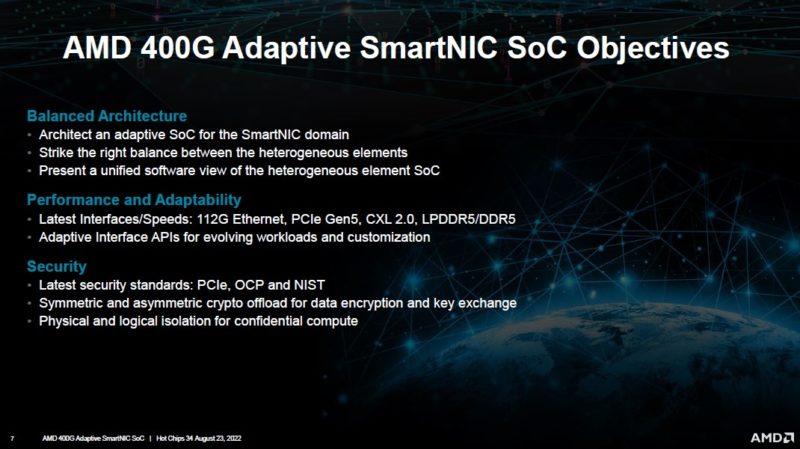
Here is AMD’s 400G NIC objectives. CXL 2.0 and PCIe Gen5 clearly show this is a next-gen product.
With the solution, AMD is targeting higher-end use cases as those tend to be where we see FPGA exotic NICs deployed.
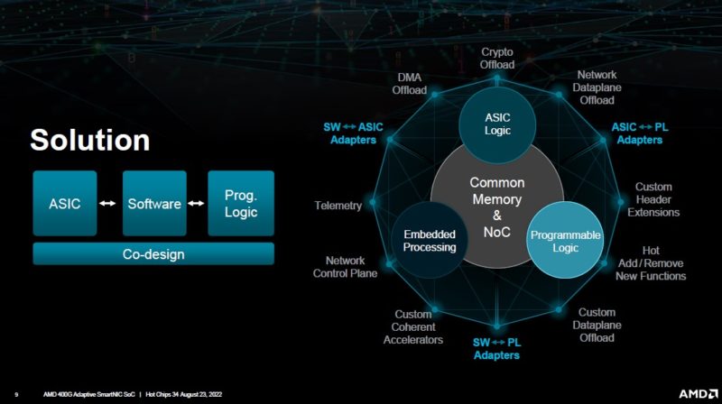
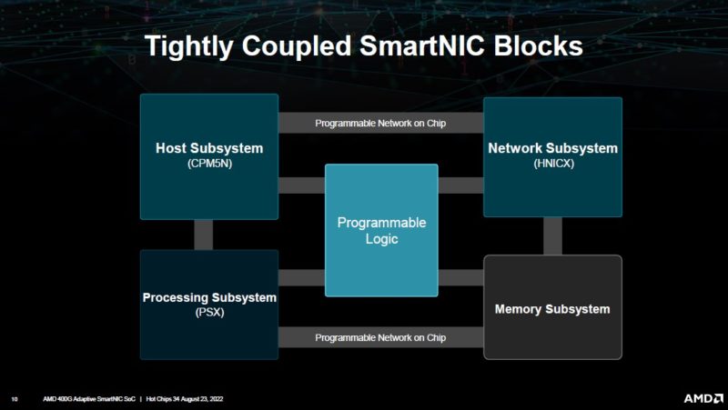
AMD has a number of devices onboard the NIC.
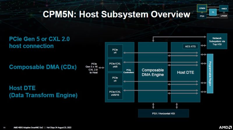
The host subsystem has PCIe Gen5 connectivity but it can also act as a CXL 2.0 endpoint.
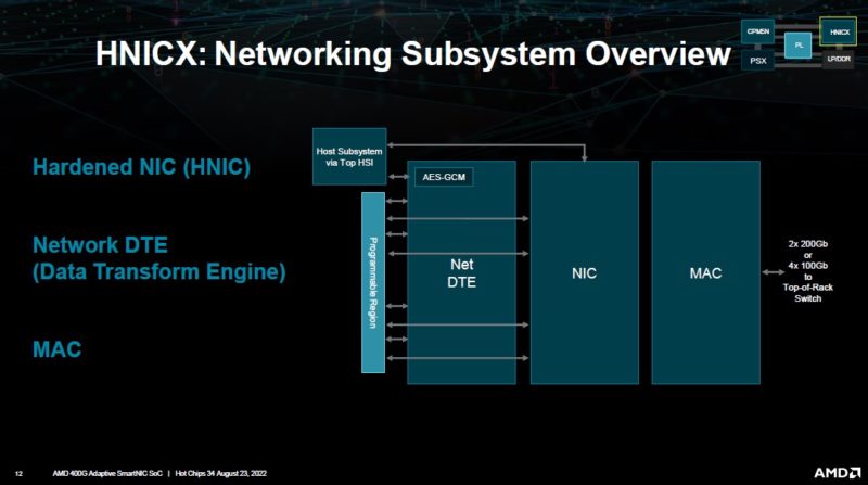
Onboard there is a hardened (e.g. not on FPGA logic) network subsystem.
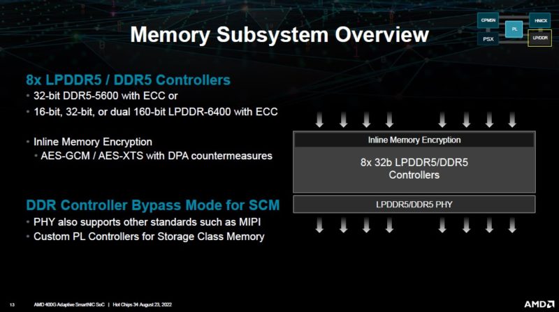
The NIC has its own memory subsystem as we would expect that uses DDR5 or LPDDR.
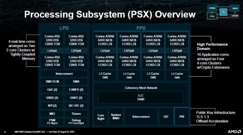
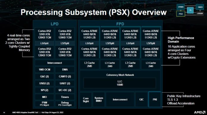
This is the processing subsystem PSX. LPD is the 4-core (Arm R52) Low Power Domain. FPD is the 8 core (Arm A78E) Full Power Domain. There are also some hardware accelerators here for things like TLS.
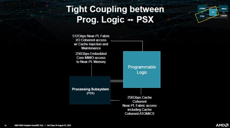
The next two slides talk about coupling between different components.
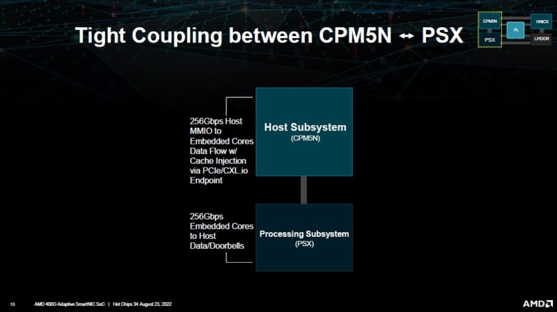
AMD says tight coupling is important for higher-speed ~400Gbps environments.
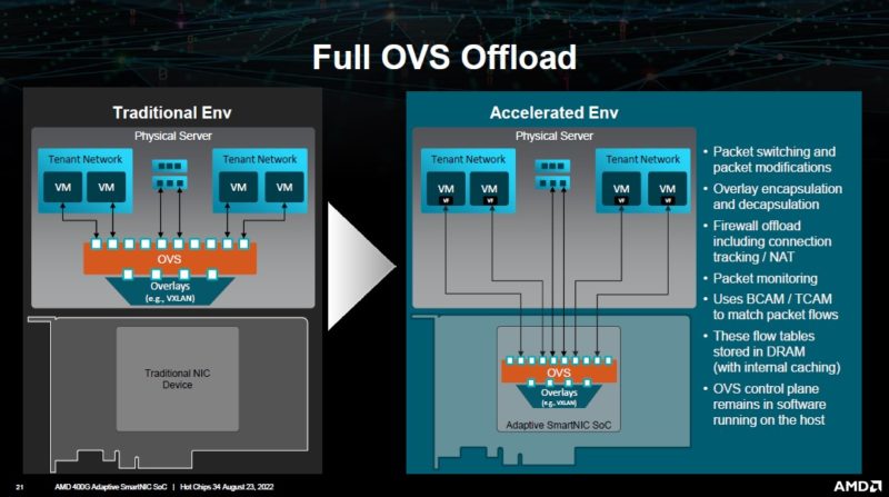
OVS is a big application for these devices. Most solutions in the space cover this.
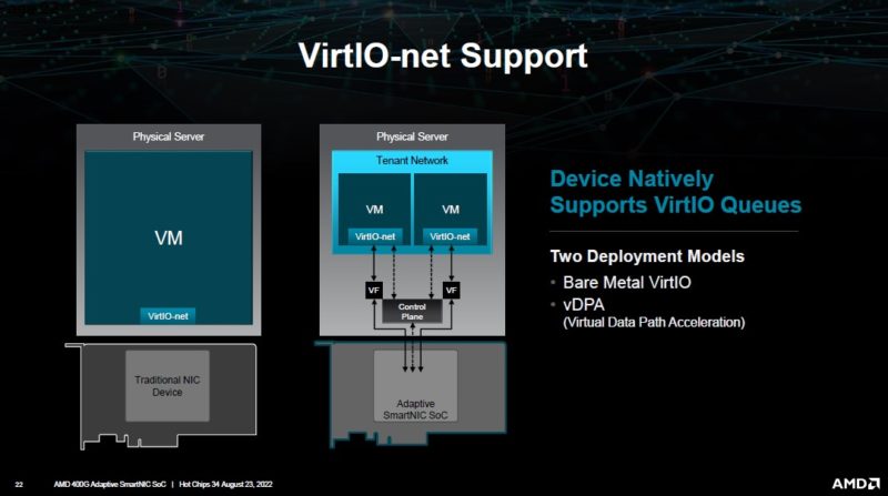
VirtIO is really interesting because it allows a cloud (public or on-prem) provider to virtualize resources and present them to tenants/ customers in a standardized way, and then manage infrastructure separately on the back-end.
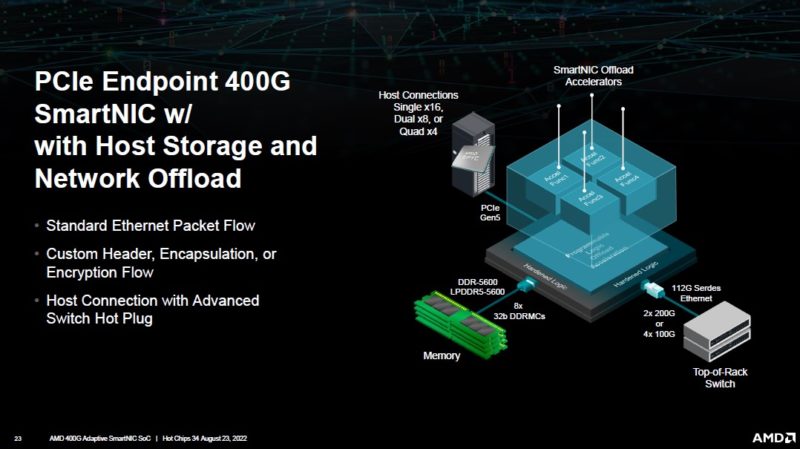
Here is a very interesting use case where there the NIC is being used for custom flows on the networking side. This is a pretty common use case.
The NIC can virtualize NVMe.
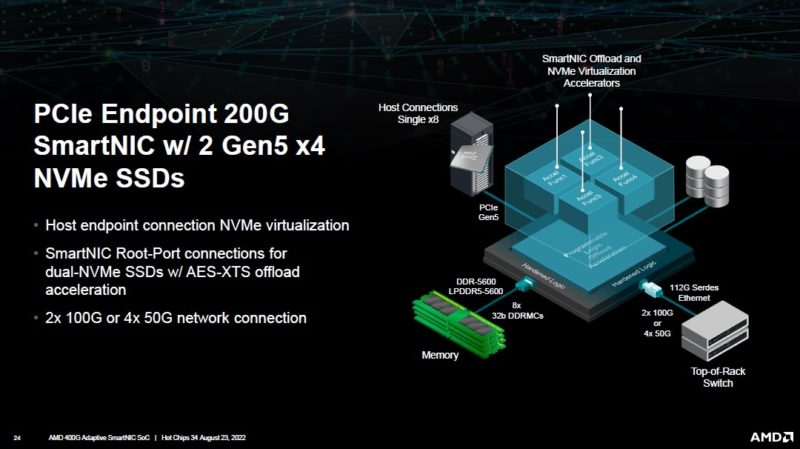
This is the solution that we showed with the Intel IPU solution in the article/ video above.
With the FPGA, this can be a PCIe root, similar to an ASIC DPU. One can then put NVMe off of the device and avoid using a traditional host.
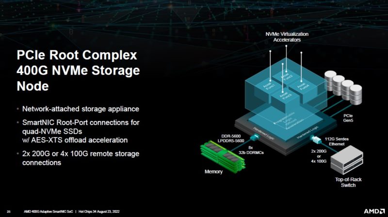
We actually showed this concept with the NVIDIA BlueField-2 DPUs a few months ago in ZFS without a Server Using the NVIDIA BlueField-2 DPU.
Here are the performance specs from AMD.
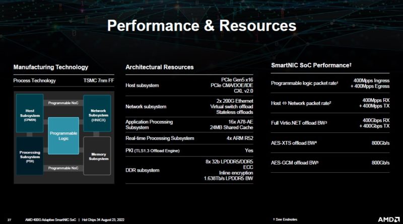
This is a fairly cool solution, but it would have been nice to see more about it in this talk.
Final Words
It is very confusing to call this a SmartNIC at this point. It is certainly something more capable than most DPUs or at least more flexible. Still, we probably need to re-brand Exotic for folks. AMD needs to address this because it now has Pensando which competes with this solution in some markets.
The card makes a lot of sense for AMD as Xilinx has a business making these types of FPGA NICs. Having a new generation is great. We were told by AMD prior to this announcement that this is not a product announcement, so this is a future product apparently. Hopefully, we get to see one live in the future, especially as AMD goes PCIe Gen5.



Hi Patrick,
Thanks for the great overview video!
Best Regards,
Chuck Sobey
General Chair, SmartNICs Summit
A slight correction: this chip has 16 application cores and four real time cores – not 12 cores. The diagram shows eight application cores for readability, and does the thing where the other two quadcore clusters are “behind” the first two.