In 2019 one of the hottest technologies is going to be Intel Optane DC Persistent Memory. This is the long-awaited marriage of 3D XPoint memory and the DDR4 memory bus. Today we have something of a sneak peek. We are going to take a 128GB Intel Optane Persistent Memory DDR4 module, and open it up. Until now, Intel Optane DC Persistent Memory has mostly been photographed with its big black heat spreader. We ended up with a handful of modules not from Intel, nor a system provider, but a handful to use. Intel announced at its Data-Centric Innovation Summit that it started shipping modules for revenue. If you are a hyper-scaler you probably already have Optane. If you are a normal enterprise, Intel does not want you to have Optane just yet. However, here we are with live modules and it is time to open them up.
Peeling Back the Intel Optane DC Persistent Memory Modules
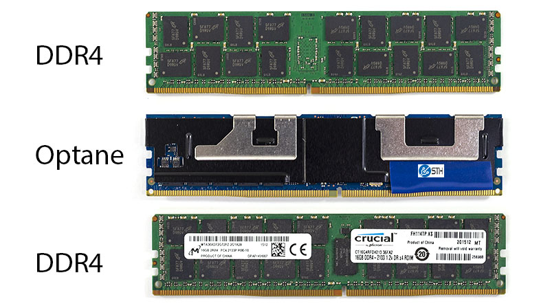
First off, we had not seen the modules side-by-side with DDR4 memory. So we grabbed two modules from the photography studio. You may have seen these modules in several STH reviews, the Micron/ Crucial DDR4 modules lasted about 6 months before they failed in different systems only three weeks apart. They were not the perfect comparison, but you can see the Intel Optane DC Persistent Memory module in the middle. All of the PCB dimensions line up with the bottom “label” side of the DDR4 sticks below:
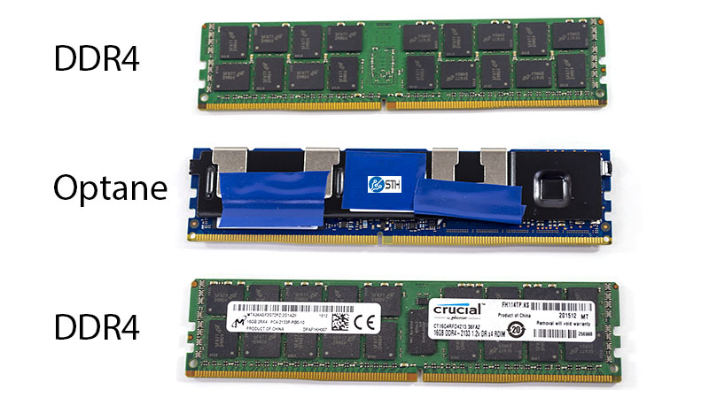
Here is the module flipped over. You can see the notches now align with the back of a normal DIMM. Other features to note are the large black heat spreader and metal clips. The STH blue electrical tape is being used to cover up the Optane DIMM markings.
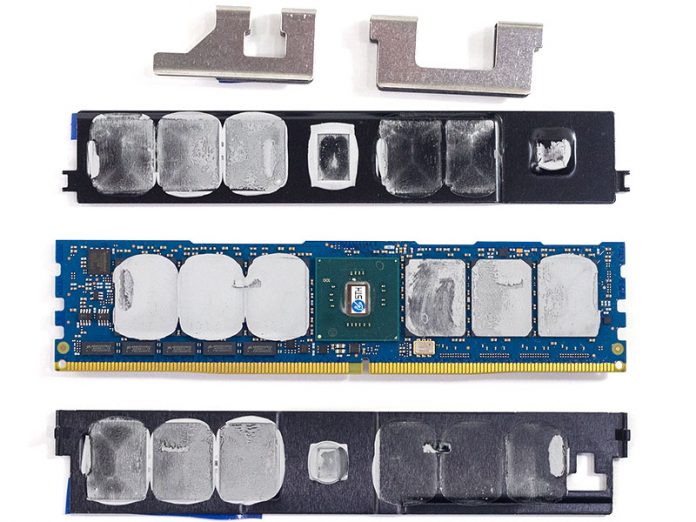
Pulling off the cover was a fairly easy affair. Simply remove the clips, then the heat spreader can be gently pried loose. We are not going to suggest you do this as the module depicted in these photos has not been confirmed to work again. You will notice a thick thermal paste. The thermal solution is far from some of the decorative solutions we have seen on some consumer parts. Intel is using some thick paste which is fairly hard. That makes sense since Intel would not want thermal paste leaking into the DDR4 socket.

One can see a total of six Optane or 3D XPoint packages flanking the Intel Optane controller on this side which would be the label side of a standard DDR4 DIMM. In the top corner, we have a Winbond IC.
On the flip side, there are five more Optane packages giving this 128GB module a total of 11 packages. This is fascinating on a number of levels. Not the least of which is that the 380GB Intel Optane M.2 NVMe SSD had only 7 packages. Intel is using 57% more Optane packages for about 34% of the capacity. Although we are not showing the package markings here, it seems like Intel may have some over-provisioning going on. It may also need more packages just to fill the memory channels. In a non-ECC DDR4 DRAM module you would expect to see 8 or 16 DRAM packages. In ECC memory you would expect to see multiples of 9 (8 data plus 1 parity.) Eleven packages is, different.
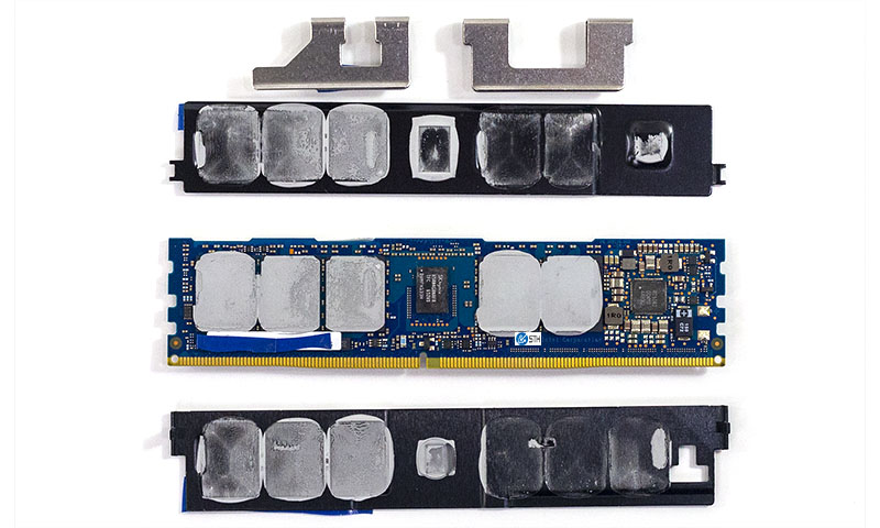
The other side also shows perhaps the most astonishing feature. On the other side of the module from the Optane controller is a DDR4 DRAM module, this one from SK.Hynix. Model number H5AN4G8NAFR-TFC. We are not sure why Intel would not use a Micron module here since Micron has been the manufacturing partner for 3D XPoint thus far.
One other feature our readers may have noticed are small rectangular chips near the DIMMs pins. We had an inclination of what these were, and double checked the markings that were bordering on microfiche size print. They are indeed Micron LRDIMM buffer chips as we can see DDR4DB02 marked on the nine chips.
Here is the video of de-lidding the DIMMs:
Final Words
It did not work on current Intel Xeon Scalable Skylake-SP parts and BIOS, nor did it work with AMD EPYC or Marvell ThunderX2 out of the box. We know Intel has the Optane Persistent Memory DIMMs working with Skylake-SP, but it looks like we are going to see this alongside Intel Xeon Cascade Lake SKUs. We expect that unless Intel feels extreme competitive pressure, it is going to reserve Optane Persistent Memory support for higher-end SKUs like Intel Xeon Platinum like it was planning to do when Intel OPM was set to launch alongside Skylake-SP.


Somehow I’m first to comment but I’ve had 5 people send this to me just from our office. Those look like they’re monster power users.
That OP looks insane. Maybe they’ve got 2 die just for extra “Oh *****” spares. Then they’re OP’ing what would be a 480GB+ SSD worth of Optane down to 128GB and using the rest for spare?
I like how these guys somehow not just find leaks but actually get hands on hardware. I’ve never seen a pic detailing under that heatsink before.
Does load reduced Optane mean you need load reduced DDR4 paired in the same channel?
We’re hoping to at least test these in a cluster this year. I still want to see how we are going to do multiple chassis mirror to persistent Optane. Proxy in front of every app?
What’s the endurance?
Exaggerated marketing by Intel: That controller is probably still just an FPGA connected to the buffers. I doubt that the optane chips are directly connected to the buffers. That explains the odd number of packages. They could have used any number (or anything).
That Winbond chip is probably NOR flash holding the FPGA’s programming.
My guess: Latencies are probably much higher than (LR)DRAM but throughput could end up being just a lil slower.
This won’t replace DRAM rather than being a better SSD.
DDR4DB02 is a jedec standard not an FBGA code. If that is all you can see on the chip that’s probably from a company like Rambus, IDT or Montage…
@Kazza, No one says Optane PM would replace DRAM, not even Intel said so. Matter of fact it can’t be run without paring with DRAM, which has been programmed that way since day one, eg: six-channel 2DPC per socket, 6 DRAMs + 6 Optane PM max.
I believe Intel sold the rest of their share to Micron, no? Do you think later on these 3D Xpoint DIMMs will come to AMD’s EPYC boards?
@Kazza you clearer did not really bother to properly read what 3D Xpoint was positioned for and you probably still don’t understand the purpose of it.
@JR @Afan Intel always went out of their way in the last two years NOT to say that this ain’t DRAM replacement for any application…
@Afan Why don’t you give us some wisdom wise man??? And no, micron is developing their own products. They are not involved in these Optane DIMMs or Xpoint DIMMs. Additionally the CPU has to be ready for these heterogeneous memory accesses and I doubt today’s EPYC is.
@JR I know that but it is was presented as an “extension” to DRAM and they actually still do:
https://itpeernetwork.intel.com/intel-optane-dc-persistent-memory-operating-modes/
“Memory Mode seamlessly brings large memory capacity at affordable cost points to legacy applications.” That’s just BS…
The “App Direct Mode” with this latency and bandwidth could have been probably done on multiple PCIeX16 interfaces instead of DIMMs allowing all DRAM channels to work at the same time as Optane. Or at least they could have added mem channels to Xeon SP. All this was due to marketing decisions.
regd that 11 chip OP … I would tend to think that since its sort of 1st Gen part, and being in DDR4 module .. it would mostly be used for write heavy tasks .. so intel is perhaps playing it safe with huge OP. it might optimise OP in next generation or after..
@JR @Afan Intel always went out of their way in the last two years NOT to say that this ain’t DRAM replacement for any application…
@Afan Why don’t you give us some wisdom wise man??? And no, micron is developing their own products. They are not involved in these Optane DIMMs or Xpoint DIMMs. Additionally the CPU has to be ready for these heterogeneous memory accesses and I doubt today’s EPYC is.
@JR I know that but it is was presented as an “extension” to DRAM and they actually still do:
https://itpeernetwork.intel.com/intel-optane-dc-persistent-memory-operating-modes/
“Memory Mode seamlessly brings large memory capacity at affordable cost points to legacy applications.” That’s just BS…
The “App Direct Mode” with this latency and bandwidth could have been probably done on multiple PCIeX16 interfaces instead of DIMMs allowing all mem channels to work at the same time as Optane. Or at least they could have added mem channels to Xeon SP. All this was due to marketing decisions.
(repost because the old one didn’t show)
virtuoso its the JDEC standard for LRDIMM buffer chips
“Byte 131 (0x083) (Load Reduced): DIMM Attributes
This byte indicates number of registers used on a module, and the type of the registers and data buffers. Further, it indicates number of rows of DRAM packages (monolithic, DDP or 3D stacked) parallel to the edge connector (independent of DRAM orientation) on each side of the printed circuit board.”
Bits 7~4
Register and Data Buffer Types
0000 = DDR4RCD01 and DDR4DB01
0001 = DDR4RCD02 and DDR4DB02
All other codes reserved