At Hot Chips 2023, Google showed off its crazy optically reconfigurable AI network. The company is doing optical circuit switching to achieve better performance, lower power, and more flexibility for its AI training cluster. The more amazing part is that they have had this in production for years.
This is being done live, so please excuse typos.
Google Details its Crazy Optically Reconfigurable AI Network
The big goal of this is to tie together the Google TPU chips.
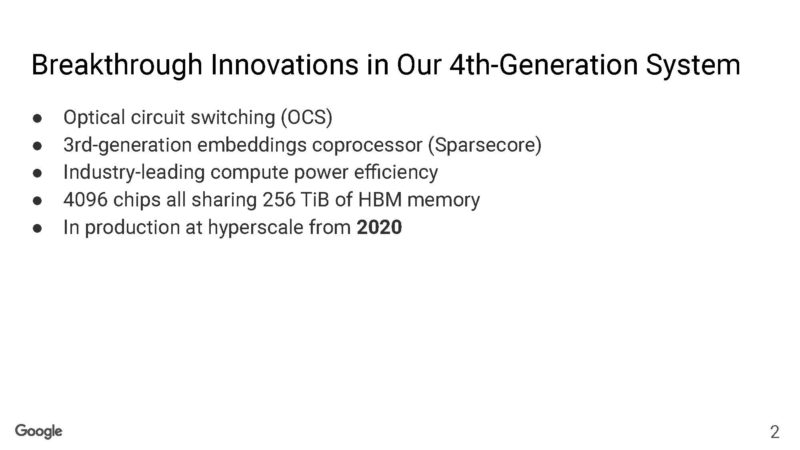
Here is the 7nm Google TPUv4. We expect this week we will start hearing more about TPUv5. Google usually can do papers and presentations about one-generation old hardware. The TPU v4i was the inference version, but this is more the TPUv4 focused talk.
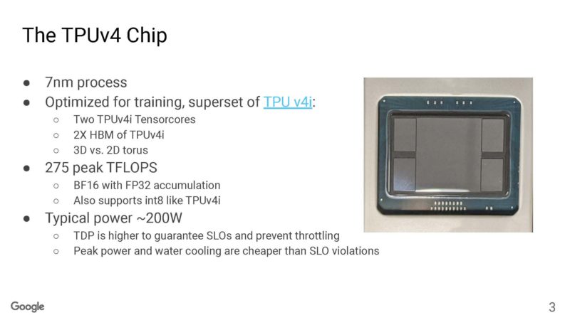
Google says it overprovisions power compared to typical power so it can fulfill a 5ms service time SLA. So TDP on the chips is much higher, but that is to allow bursting to meet those SLA bursts.
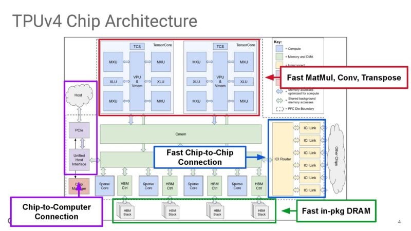
Here is the TPUv4 architecture diagram. Google builds these TPU chips not just to be a single accelerator, but to scale out and run as part of large-scale infrastructure.
Here is the Google TPUv4 versus TPUv3 stats in one of the clearest tables we have ever seen on this.
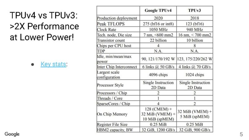
Google has more than doubled the peak FLOPS, but reduced the power between TPUv3 and TPUv4.
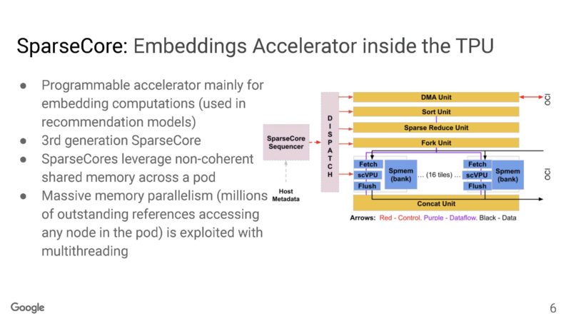
Google has a SparseCore accelerator built into the TPUv4.
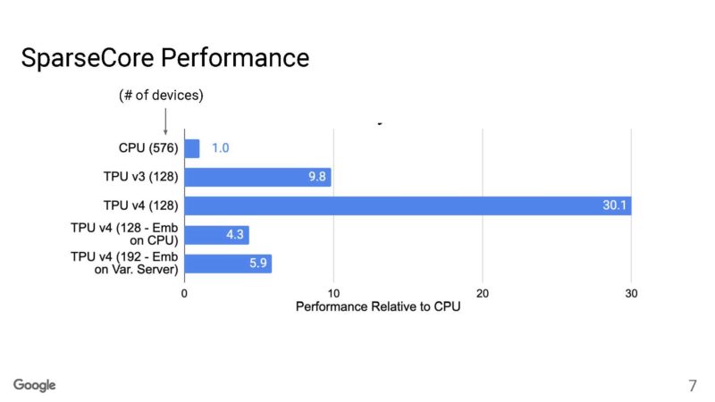
Here is Google’s TPUv4 SparseCore performance.
The board itself has four TPUv4 chips and is liquid-cooled. Google said that they had to rework data centers and operations to change to liquid cooling, but the power savings are worth it. The valve on the right controls flow through the liquid cooling tubes. Google says it is like a fan speed controller, but for liquid.
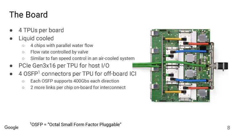
Google also says that it is using PCIe Gen3 x16 back to the host since this was a 2020 design.
Google has power entering from the top of rack like many data centers, but then it has a number of interconnects. Within a rack, Google can use electrical DACs, but outside of a rack, Google needs to use optical cables.
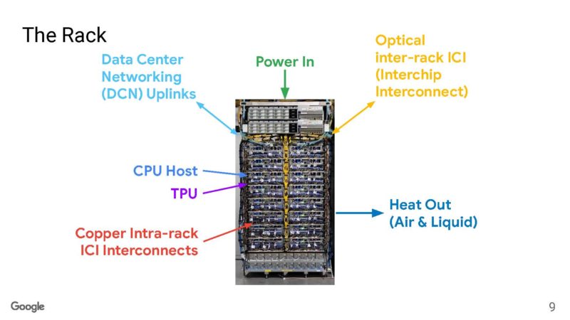
Each system has 64 racks with 4096 interconnected chips. For some sense, NVIDIA’s AI clusters at 256 nodes have half as many GPUs.
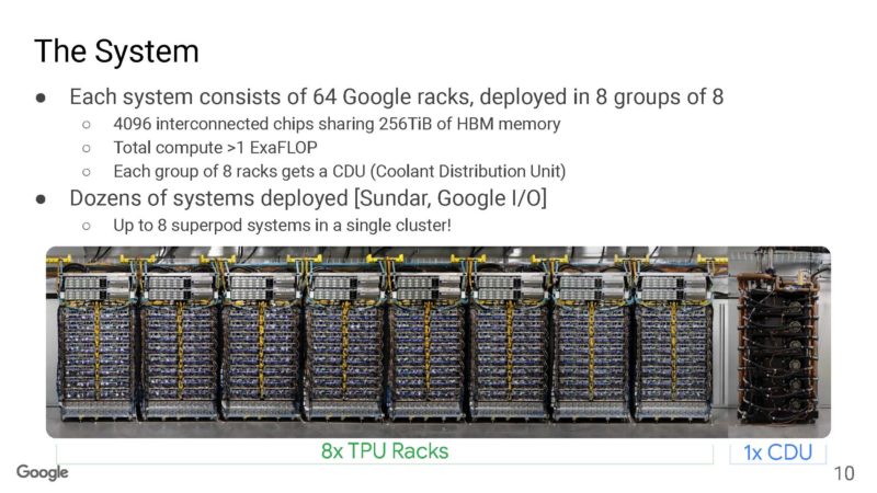
Also at the end of the racks, we see a CDU rack. If you want to learn more about liquid cooling, you can see our How Liquid Cooling Servers Works with Gigabyte and CoolIT. We are going to have more liquid cooling content soon. Google says the flow rates of liquid are higher than water in a hook and ladder firetruck’s hose.
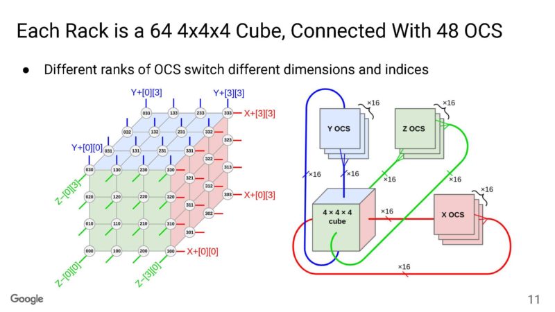
Each rack is a 4x4x4 cube (64 nodes) with optical circuit switching (OCS) between the TPUs. Within the rack, the connections are DACs. The faces of the cube are all optical.
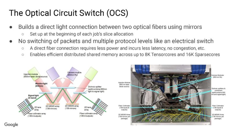
Here is a look at the OCS. Instead of using an electrical switch, using the OCS gives a direct connection between chips. Google has internal 2D MEMS arrays, lenses, cameras and more. Avoiding all of the networking overhead allows sharing of data more efficiently. As a quick aside, this in some ways feels akin to DLP TVs.
Google said that it has over 16,000 connections and enough distance of fiber in the super pod that it can encircle the state of Rhode Island.
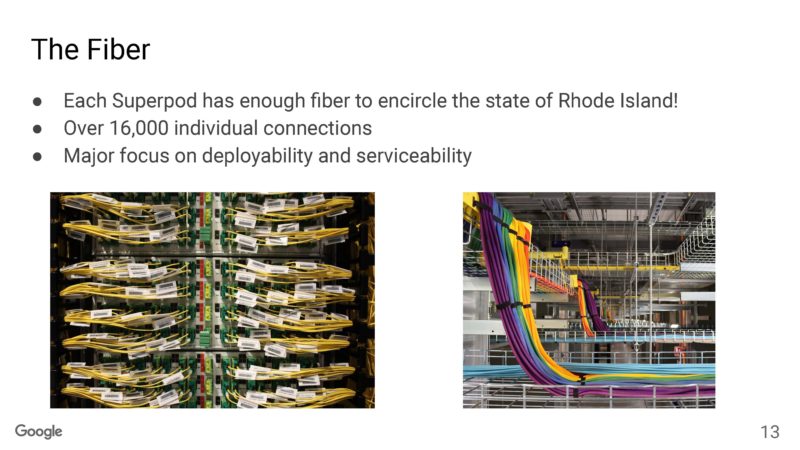
Because there is so much point-to-point communication, it requires a lot of fiber strands.
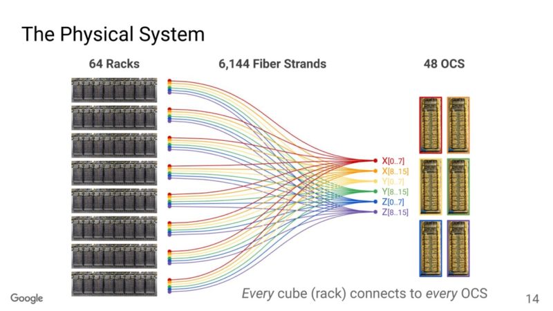
Beyond that each pool can be connected to larger pools.
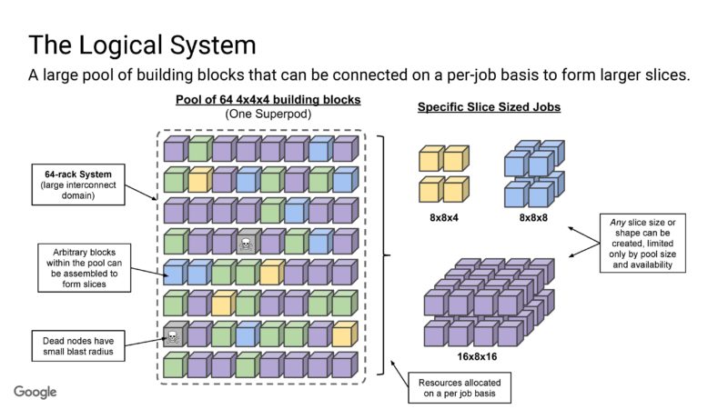
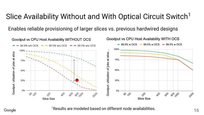
The OCS, because it is reconfigurable, can yield higher utilization of the nodes.
Google can then change topologies by adjusting the optical routing.
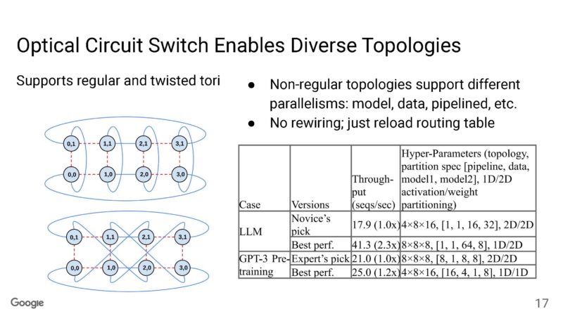
Here Google is showing the benefit of different topologies.
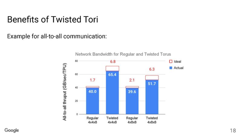
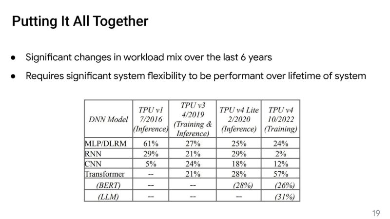
This is important since Google says that the changes in model needs can drive system changes.
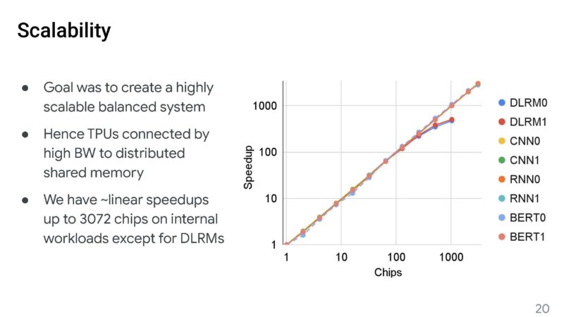
Here is Google’s scaling on a log scale with linear speedups on up to 3072 chips.
Google also increased the on-chip memory to 128MB to keep data access local.
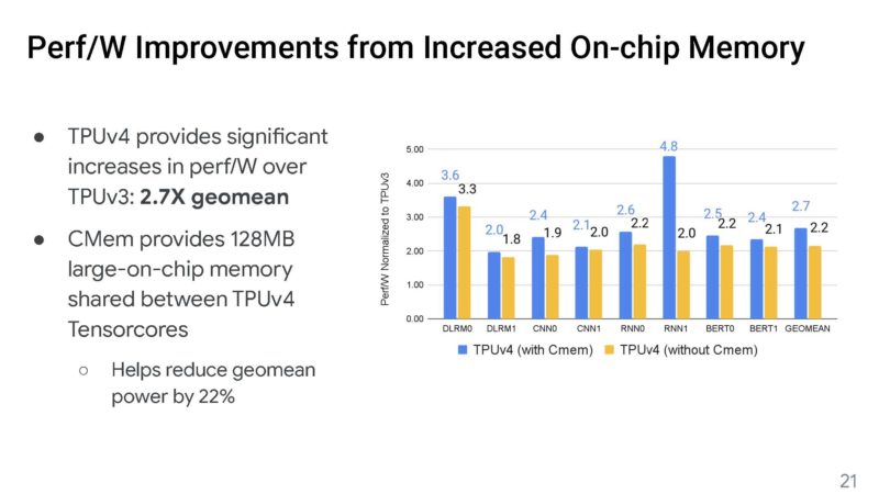
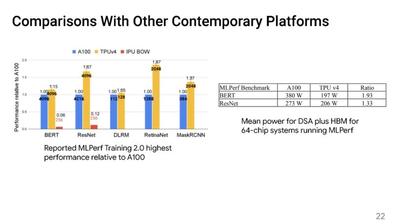
Here is Google’s comparison against the NVIDIA A100 on a performance-per-watt basis.
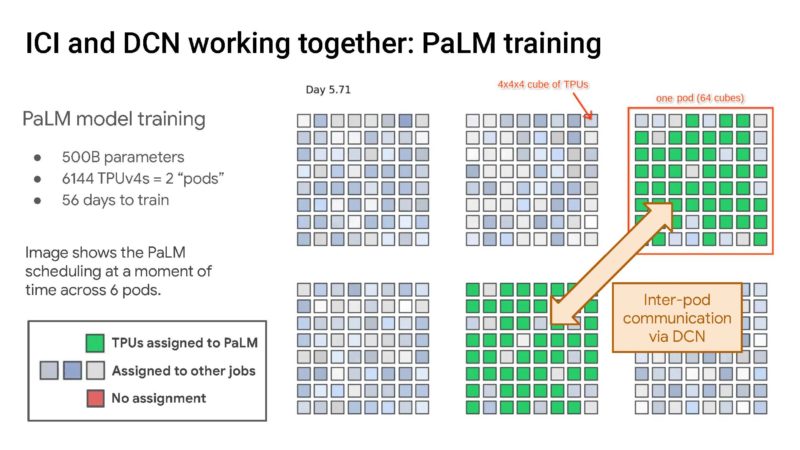
Here is the PaLM model training over 6144 TPUs in two pods.
That is a huge number!
Final Words
It is about time for Google to start talking about the TPUv5, and it happens that Google NEXT is this week. Still, this optical interconnect is a really innovative technology.
Something that is pretty clear now, is that Google is solving large problems with huge infrastructure. It has the opportunity to push into the AI space more. It is just a question of how fast Google will start pushing its AI hardware and cloud services against NVIDIA while also needing to buy NVIDIA GPUs for its customers using those instead of TPUs.


Actually a lot of things they presented is already implemented on Fugaku with a larger scale, so it is not a big surprise that this is in production for years.