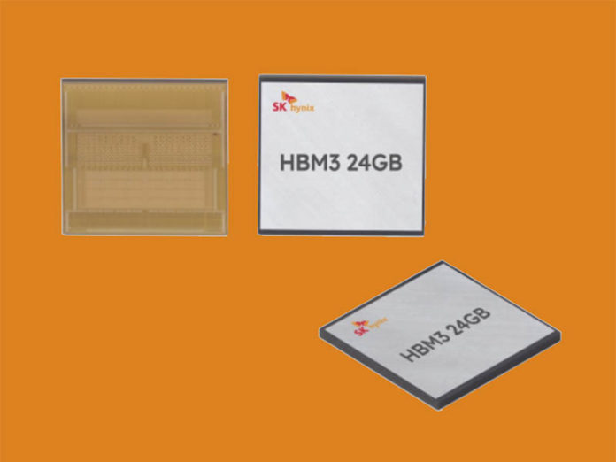
SK hynix has a new process to allow for larger capacity HBM3 modules. The new 12-layer technology means that the company has up to 24GB stacks of memory, a 50% increase over the previous generation’s 16GB stacks.
SK hynix Introduces New 12-layer HBM3 Memory
One of the big challenges with adding more layers to a HBM3 stack is the height. If the stack changes in height, then it means that advanced packaging methods may need to change in order to fit the new memory moudules onto chips and substrates.
To counter this, SK hynix says its engineers used Advanced Mass Reflow Molded Underfill (MR-MUF) technology for the latest generation along with Through Silicon Via (TSV) technology. That means that each DRAM chip is thinner, allowing for a 24GB capacity in the same height as the previous generation’s 16GB stack.
While TSV technology is used in many chips these days, if you are not familiar with MR-MUF or Mass Reflow Molded Underfill SK hynix describes it as: A method of placing multiple chips on the lower substrate and bonding them at once through reflow, and then simultaneously filling the gap between the chips or between the chip and the substrate with a mold material. (Source: SK hynix)
This new generation improves upon the 8-layer HBM3 product at 16GB with 12-layers at 24GB of capacity.
Final Words
SK hynix says that it has already shipped samples to a number of customers. This type of technology is what allows GPUs like the NVIDIA H100 and others to increase memory capacities. Increasing memory allows for things like more data to be stored on-chip, and on HGX H100 baseboards limiting access to off-chip or off-NVLink data. Of course, many other vendors use HBM stacks in accelerators so it is far from just a NVIDIA-only technology. Still, increasing capacity in the same footprint will help to build higher memory devices.


