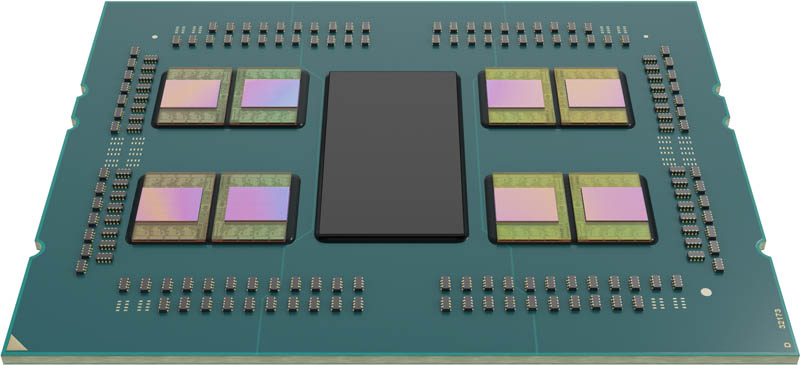
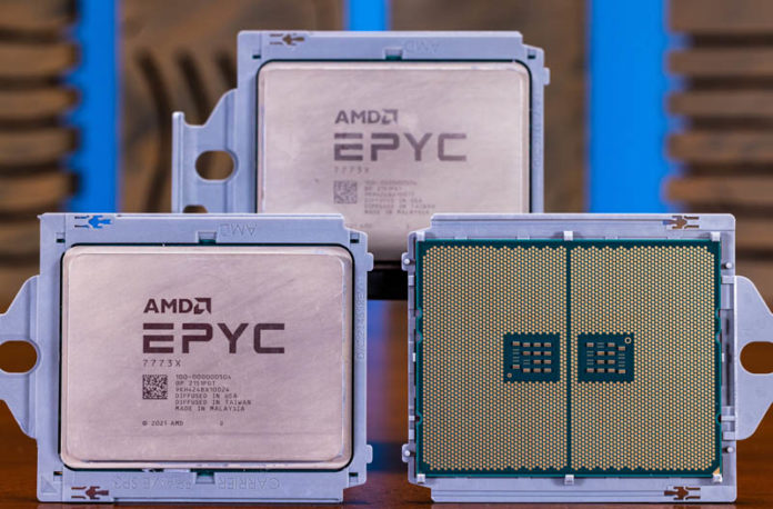
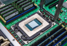
Today we finally get to share details of the AMD EPYC 7003X series, dubbed “Milan-X”. In short, AMD Milan-X takes the classic EPYC 7003 “Milan” CPUs, stacks an extra half a GIGABYTE of L3 cache on top, and sheds some small amount of frequency capacity. This is AMD’s equivalent of swapping a really good Friday night local band with the Foo Fighters, Beyonce, Taylor Swift, or something like that. Either way, bar patrons are going to come away talking about music, but going with the A-list celebrity is the show people will talk about for years to come. AMD is having its Taylor Swift moment with Milan-X.
We have a video for this one (that was a few hours late):
We have a special guest with Wendell from Level1Techs talking about the new chips since we were both at AMD in Austin for the briefing. As always, we suggest opening this in a new browser, tab, or app for the best viewing experience.
A quick launch day note: We have a few other screenshots that will be added to this over the coming days. This was being done on a crazy short timeframe, with the GTC 2022 keynote tomorrow, so a few resources are not yet ready. We cut a huge amount from this article to have it ready for the embargo, but it was not enough apparently.
Some Quick Background
On STH, many times we see new SKUs announced and it is some variation of new clock speeds and core counts. When AMD EPYC 7003 “Milan” was announced, it was a generational improvement with higher IPC due to core changes and unifying the chiplet L3 cache. If you had the AMD EPYC 7002 “Rome” series, you could get improvements, but the upgrade path was more likely from the EPYC 7001 “Naples” generation or from Xeons. The new Milan-X parts are so good, that a portion of the Microsoft Azure Cloud is ripping out its existing EPYC 7003 and replacing it with the EPYC 7003X series because it offers that much more performance. Usually, cloud providers just add nodes and create new instance types. Milan-X is so transformational that Azure’s HPC team is doing a rip-and-replace of its current generation. At the same time, it is certainly not going to be the CPU for every workload. As a result, the thought was to get to testing, then come up with the best recommendation we could based on what we saw.
Just to be 100% frank here, we had fewer than 6 days to do this entire piece, while still doing our normal STH site duties plus gearing up for NVIDIA GTC this week. Our benchmark suite takes longer than 7 days to run and that is without verification of the results. We also needed to take photos, flash the bios on systems, and so forth. All told, there was not a ton of time to test these, but I think we have a good handle on how to explain the new chips. Most likely that will mean we have a follow-up, but that is just the nature of the timing on this one.
In this article, we are going to discuss how Milan-X is made. We are then going to show the performance and what this entire thing looks like. Finally, I want to spend some time discussing the market impacts of a chip like this because there is more to unpack than meets the eye.
AMD Milan-X: How it is Made
For some context regarding what AMD Milan-X is, and is not, let us get into how it is made. We are not going to absolute depth on this, but it is important to understand why it is different. One of the big drivers is that silicon scaling has diverged significantly between analog (a lot of the I/O), SRAM (cache), and logic. As a result, we see things like AMD creating an I/O die in its EPYC processors to start putting different parts of silicon on process nodes that make sense for these curves. To be clear, Intel is also following this trend and vision, AMD is just shipping GA parts with its methodology.
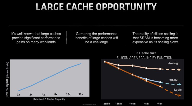
With the I/O die separated out, that leaves the Zen 3 CCD. Each CCD can have up to eight cores and 32MB of L3 cache. The challenge though is that adding SRAM to the die is not as efficient. So, AMD did something different, it started stacking chips.
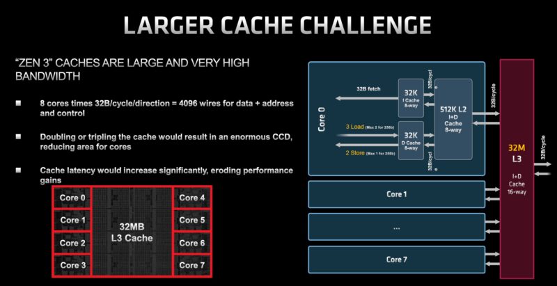
AMD is leveraging 3D, or is effectively stacking chips vertically instead of simply adding more chips to a 2D/ 2.5D footprint in a horizontal plane.
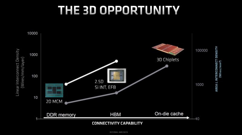
To do this, AMD is adding a 64MB L3 cache chiplet to each of the eight CCDs in Milan-X. All four of the Milan-X SKUs have eight CCDs.
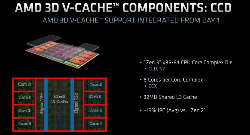
Each of these 64MB cache chiplets uses TSVs to connect to the CCD and is stacked atop the 32MB of the existing CCD cache. Then additional fillers are added to each side for structural rigidity as well as thermal transfer from the compute cores to the package and eventually the thermal solution. As a quick aside, the EPYC 7002 Rome CCDs had the potential to use 3D V-Cache, but the manufacturing technology was not quite ready for it.
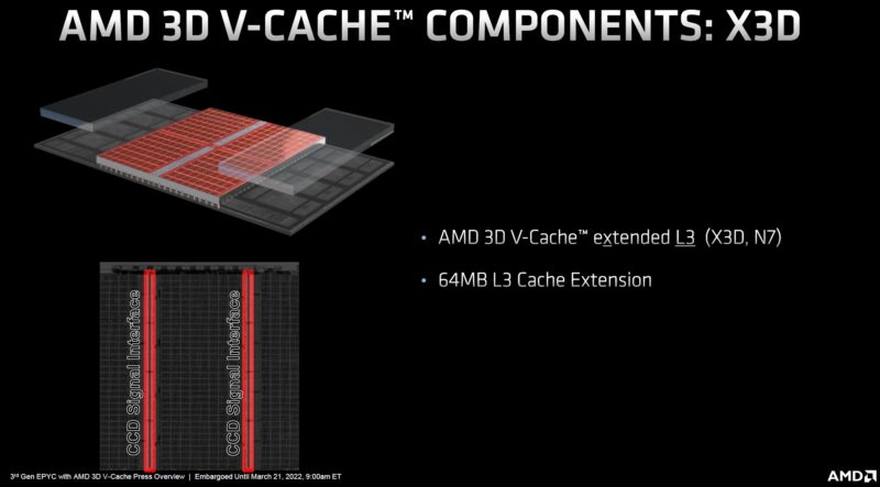
Stacking one die atop of another die is challenging because features need to align during manufacturing, they need to be small and high performance to be low power. They also have to account for details like different rates of thermal expansion between the silicon and other sandwiched materials. This is not like stacking Lego bricks as much as that is an easy visualization. At its core, this is a tough engineering problem.
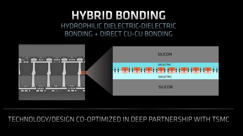
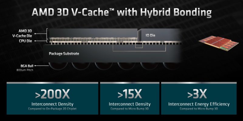
With this, AMD is using hybrid-bonding using copper-to-copper connections via TSMC SoIC.
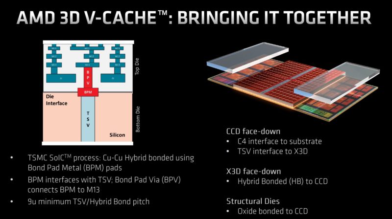
AMD has a nice cross-section just showing how dense this approach is. For reference, we can see the I/O die and the CPU die that we have basically seen since Rome. We see the BGA package balls on the bottom of the chip. One can see the density of the CCD to SRAM connectivity.
Many of our readers care less about the manufacturing and more about the “so what”. Here is basically the difference: it triples the amount of L3 cache that each CCD, with 2-8 cores, can access locally.
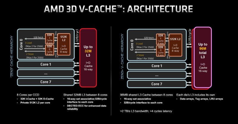
Local cache means avoiding trips to main memory that requires going off of the CCD to the I/O die, then out across the motherboard to main memory.
Some commentators are going to cite that there is a very small latency hit just for the clock cycles to go up through the TSV structures to the 64MB cache die. The real-world impact is that the base 32MB of L3 is still present. The additional 64MB of L3 cache is an order of magnitude faster than going out to DDR4 to where the latency is negligible. The real comparison in terms of speed, latency, and power is from on-CCD versus DDR4, not a low single-digit clock cycle hit to access the extra L3.
Next, let us get to the SKU stack to see the options to actually get a chip using this technology.


This is excellent. I’m excited to get a r7525 with these and try them out. I sent this to my boss this morning and he OK’d ordering one so we can do profiling on our VMware servers
@cedric – make sure you order it with all the connectivity you’ll ever want. Dell has been a bunch of [censored] when we’ve opened cases about bog-standard Intel X710 NICs not working correctly in our 7525s. So much for being an open platform.
Not that I’m bitter.
Why the 7373X with 16c is more expensive than the 7473X with 24c ?
flo it’s because it has fewer cores so its cheaper to license.
Now that the 7003x “shipping”, perhaps they can get around to shipping the 7003 in bulk. I’ve got orders nearly 9 months old.
While per-core licensing costs seem to be a consideration for some people, I think this kind of optimisation is only possible because certain proprietary licensing models need updating to account for modern computer hardware. Given the nonlinear scaling between frequency and power consumption, it appears environmentally backwards to base hardware choices on weird software licensing costs rather than performance per watt or something similar that neglects arbitrary licensing constraints.
On another note, NOAA open sourced their weather forecasting codes a few years ago and WRF (based on models developed by NCAR) has been open source for much longer. I think the benchmark problems associated with these applications would make for an interesting journalistic comparison between new server CPUs with larger cache sizes.
@Eric – Environmentally backwards, possibly, but so often the hardware platform is the cheapest part of the solution – at least in terms of capital costs. I don’t think it’s necessarily unreasonable to optimize for licensing costs when the software can easily dwarf the hardware costs–sometimes by multiple orders of magnitude. To your point though, yes, the long-term operational expense, including power consumption, should be considered as well.
The move to core-based licensing was largely a response to increasing core counts – per-socket licensing was far more common before cores started reaching the dozen+ level. Hopefully you’re not advocating for a performance/benchmark based licensing model…it’s certainly been done (Oracle).
Lilu Dallas multipass :)
ok, so Taylor Swift has a Cache of 768Mbytes? I never woulda guessed :).
I find the speedups in compilation a bit underwhelming. My hunch is that the tests are performed the usual way – each file as a separate compilation unit. I work on projects with tens of thousands of C++ files and the build system generates files that contain includes for the several hundred cpp files each and then compiles those.
When you have a complicated set of header files, just parsing and analyzing the headers takes most of the compilation time. When you bunch lots of source files together you amortize this cost. I guess in such scenario the huge L3 cache would help more than for a regular file-by-file build.
Dell submitted SAP standard application benchmark, comparing 2 x AMD EPYC 7773X with 2 x AMD EPYC 7763 processor. Milan-x is able to show 14% increased in benchmark while serving 11,000 more users.
https://www.sap.com/dmc/exp/2018-benchmark-directory/#/sd?filters=v:4a9e824336e2837bf9081e423d579859;v:4a9e824336e2837bf9081e423d58f740;v:4a9e824336e2837bf9081e423d5a63e6
What happened to the Stockfish Chess Benchmark?