On the calendar for this week, we had a piece set highlighting the complexity of Intel Optane DIMMs. As many have seen, at STH we have been using Optane SSDs as database storage for years, and the next step was going to be Intel Optane DIMMs. As we started going from slides and presentations, to actually operating Intel Optane DCPMM (or PMem 100) and with PMem 200 being a key driver for Cooper Lake, it was time to bridge slideware to practical experience. Then, hours before that piece was going live, Micron announced that it was exiting the 3D XPoint business and selling its Lehi, Utah fab that makes the media.
As a result, we pulled the original piece to augment it with what and why Micron we think is making that announcement. In hindsight, it probably should have been two articles. At the same time, we are getting into a level of detail around Intel Optane Persistent Memory that is beyond most slideware, but also above many detailed whitepapers. As such, the complexity we planned to show in the original piece actually helps explain part of Micron’s decision.
Video Version
Since we have a lot to share, we also have a video version accompanying this article. A few mid-week edits later, and it mostly matches what we will cover in this piece, just in video form for those who prefer to listen.
As always, we suggest opening this in a separate browser tab to get the best viewing experience.
The Quick Intel Optane / 3D XPoint Background
For a bit of background, with Intel Optane (the company’s marketing name for 3D XPoint-based products) we effectively get a cross somewhere between DRAM and NAND. Typically, this is described as byte-addressable non-volatile memory. The basic idea is that it is a persistent storage solution, similar to NAND flash that is in your SSD, and DRAM memory that is the RAM in your PC. When you hear a PC has say 16GB of RAM and a 256GB SSD, you can think of Optane as a cross between the two, but that is a very simplistic view, so let us get into a bit of what is going on. In practice, it operates differently than many who have not used Optane PMem understand so we wanted to clear that operations part up.
First off, the 3D XPoint media has a cell density between that of DRAM and NAND. As a result, the idea is that we can get higher DIMM capacities than with DRAM. At the same time, the structures storing data are larger than NAND, so we get less capacity than NAND. This has a direct relationship with the manufacturing cost. As an in-between product, 3D XPoint needs to stay somewhere in the middle since it is not always superior to DRAM (DRAM is faster) and it is also not always superior to NAND (NAND is higher capacity.) As a result, as a direct replacement to either, 3D XPoint needs to be somewhere in the middle unless a unique value proposition is offered.
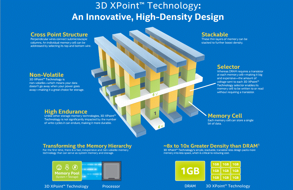
Second, in terms of endurance and performance, Intel’s Optane based data center products are rated for effectively unlimited endurance. This is an exaggeration in some ways, but the endurance ratings are so high that, unlike with NAND, endurance is not a concern. Furthermore, an Optane SSD typically writes directly to media, instead of a write going first to DRAM then to media. That intermittent write to DRAM is basically why the industry cares about power-loss protection for data center SSDs. If the power fails mid-write, then DRAM loses contents which means data written to a NAND SSD is not safe until it makes it to the NAND. For write logs, such as a ZFS ZIL/ SLOG and databases, this is absolutely magic.
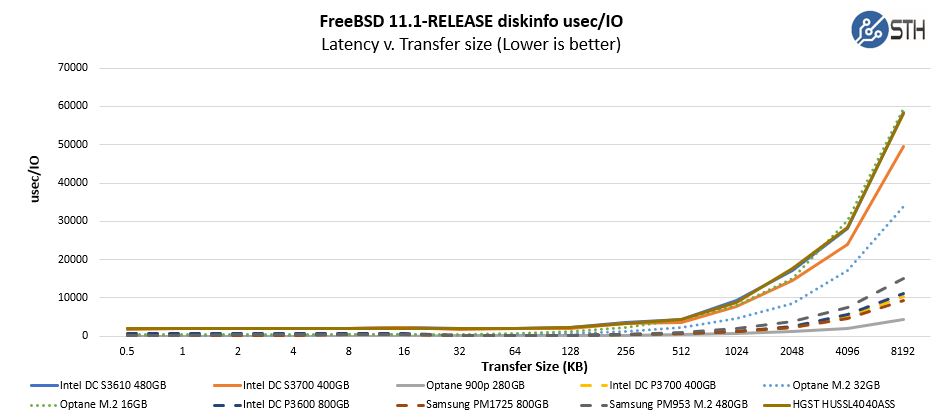
The byte-addressability is a big difference compared to today’s common QLC NAND. In terms of performance, compared to NAND, 3D XPoint is much faster in solutions, especially at low queue depths, and has a better quality of service because it is byte-addressable.
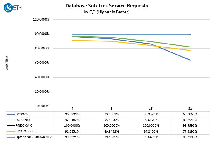
At the same time, performance-wise, 3D XPoint is still an in-between solution, so not everything is perfect. It is slower in two ways compared to DRAM typically found in your DIMM sockets. First, it has a higher latency because it is writing to the persistent 3D XPoint instead of DRAM. The second is one that not many discuss. The first two generations of Intel Optane DCPMM or PMem 100 and PMem 200 operate at DDR4-2666 speeds with Cascade Lake and Cooper Lake.
That is extremely important. Once you add PMem to a server, the memory speed drops to DDR4-2666. So on Cascade Lake or the 2nd generation Intel Xeon Scalable that means we go from 6x DDR4-2933 per socket to 6x DDR4-2666. The same happens with the DDR4-3200 3rd Gen Intel Xeon Scalable CPUs as well. Compared to modern CPUs such as the AMD EPYC 7002/ 7003 series and the Ampere Altra as examples, those are both 8x DDR4-3200. So theoretically, even when we compared 2nd Gen Xeon Scalable with PMem 100 to without, we only lost around 9-10% of bandwidth in our conceptual model in the table below:

Theoretical bandwidth plummets when using DCPMM/ PMem compared to the 8-channel DDR4-3200 solutions that have been in-market since at least 2019 with AMD EPYC 7002 “Rome”. Effectively, the Intel-only DCPMM / PMem modules added to a system create a memory bandwidth deficit with Cascade Lake/ Cooper Lake CPUs. This, combined with almost dizzying memory channel population requirements (so long we removed from this piece and an 8-minute segment from the already long video) means that just adding the PMem to a system has impacts beyond those of DRAM and NAND.
Very few folks discuss the memory speed impact, but it is real, and it is very easy to understand what is happening.
So why would one lose memory bandwidth, and get less capacity storage, to add Optane? The answer is to get a mixture of both. To look at this, we need to understand what Optane is effectively doing when we add PMem modules.
Intel Optane DC Persistent Memory (PMem) Real-Life Modes
The name of this section is chosen specifically because this is how Intel often simplifies Optane to show what is going on. Intel shows Memory Mode and App Direct mode. That sounds great, but in the application, it is full of glorious complexity. When I first saw the slides, then saw the configuration settings on systems, it took a while to figure out what was happening. To Intel’s credit, they do have documentation on all of this, and it is more complex than what we are going into here, but I wanted to give some sense of another layer down of complexity.
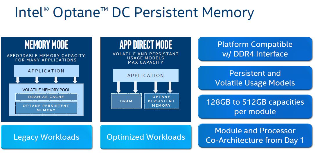
First, one can see Memory Mode and App Direct Mode. Memory Mode is the one that is perhaps the easiest to understand and sell. Indeed, I heard a lot of the early adoption was for memory mode, and we are now using this in the STH hosting cluster, but we are going to come back to that.
Memory Mode: Conceptually Easy, Complex Implementation
Intel says Memory Mode uses the Optane PMem as memory, effectively as a substitute for adding more expensive DRAM. That is a high-level abstraction, and it somewhat works. I am going to offer another model which fits with the slide above but may seem strange to those who have not gotten into the details. Instead of thinking of PMem as DRAM, think of PMem like a storage array where you have data on SSDs, but then cache the frequent data in a systems DRAM or RAID controller DRAM. That means frequently accessed data hits fast DRAM, then is periodically flushed to the underlying storage. If you are worried at this point about storing data on “memory modules” then Intel’s answer is that there is a cryptographic key that is reset every reboot so the data on the modules is so encrypted one cannot just take the modules out of a system and access the data. Everything is effectively gone every reboot.
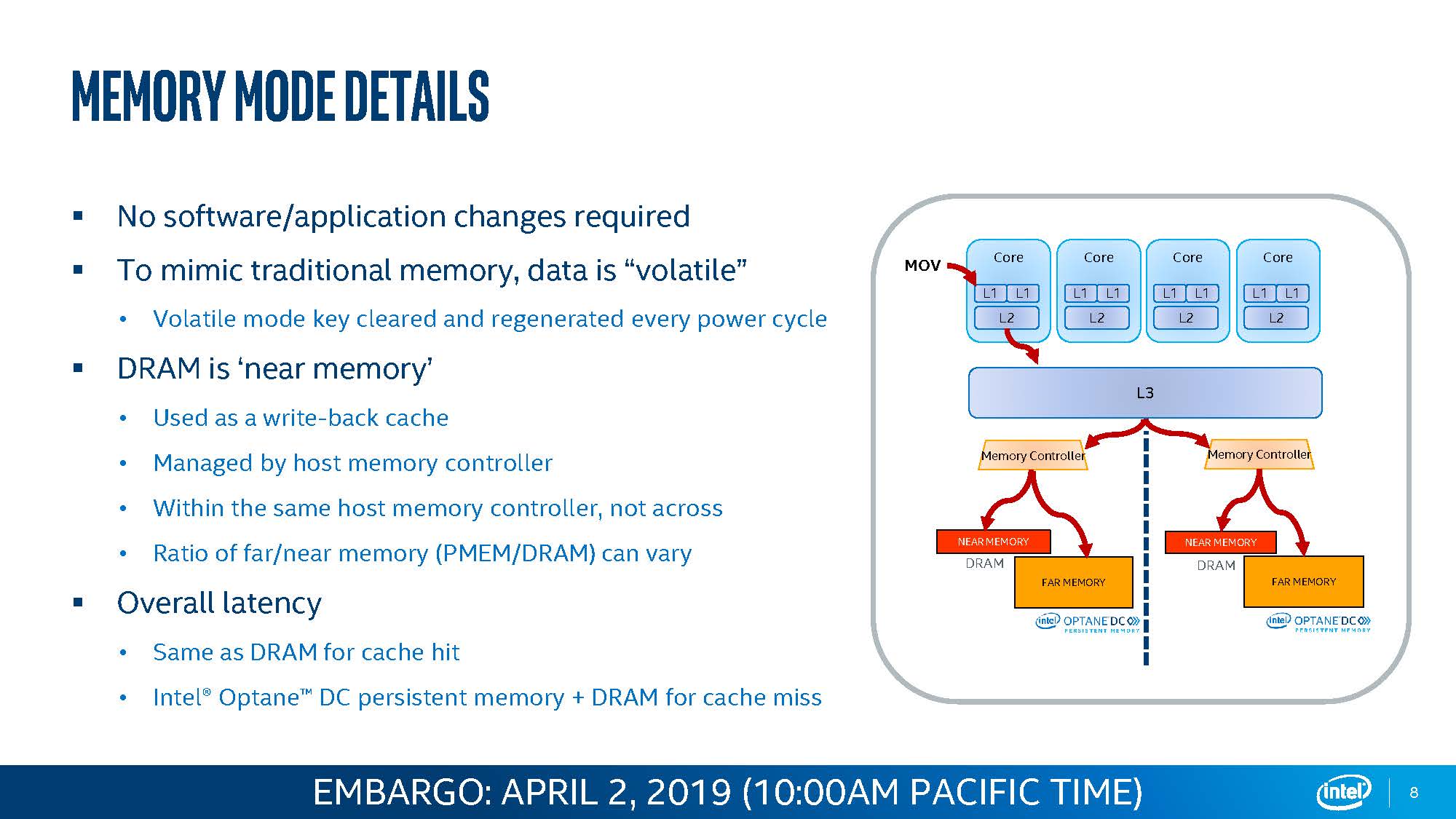
As a result, one needs to add memory alongside Optane. For performance, Intel recommends a 4:1 ratio so effectively there is around 25% as much DRAM as Optane. It turns out that there are a number of research papers by hyper-scalers that show that often servers only have maybe 20-40% of data as hot, and the rest is relatively cold. In other words, around a quarter of data needs to be in DRAM while the remainder can be in something a bit slower, in this case, Optane PMem.
That ratio is a big challenge though. For example, if one wants to use 128GB DIMMs with a 4:1 ratio, then one needs to populate a 32GB RDIMM and a 128GB PMem module in the same memory channel. As a result, the cost of the 32GB RDIMM plus 128GB PMem needs to be less than 2x 64GB which would offer the same capacity and higher performance. In our hosting nodes, we tend to use 16GB + 128GB because that tends to work well and is a lot less expensive when scaled across 24 DIMM slots in a system. Just for a sense, we save a few thousand dollars per node with little impact on our hosting performance with this solution.
Intel’s challenge and this gets to the profitability, is that for Memory Mode pricing is constantly pressured by DRAM pricing, especially when DRAM prices fall. Memory pricing is more volatile, Optane PMem pricing needs to be more volatile as well. Memory Mode may be easy to understand, and easy for adoption, but it is constantly bound by needing to provide a discount to DRAM-only configurations.
The Persistent Bit: App Direct Mode
The way Intel gets to more value is with App Direct Mode. The easiest way to think of App Direct Mode is that you are turning each of the PMem modules into a SSD. Then comes the complexity. One way App Direct Mode can be used is via APIs with applications that support PMem. If an application is aware, such as SAP HANA, then the application can write to the PMem modules as if it is a super-fast storage tier. If the application is unaware, then there is a fallback.
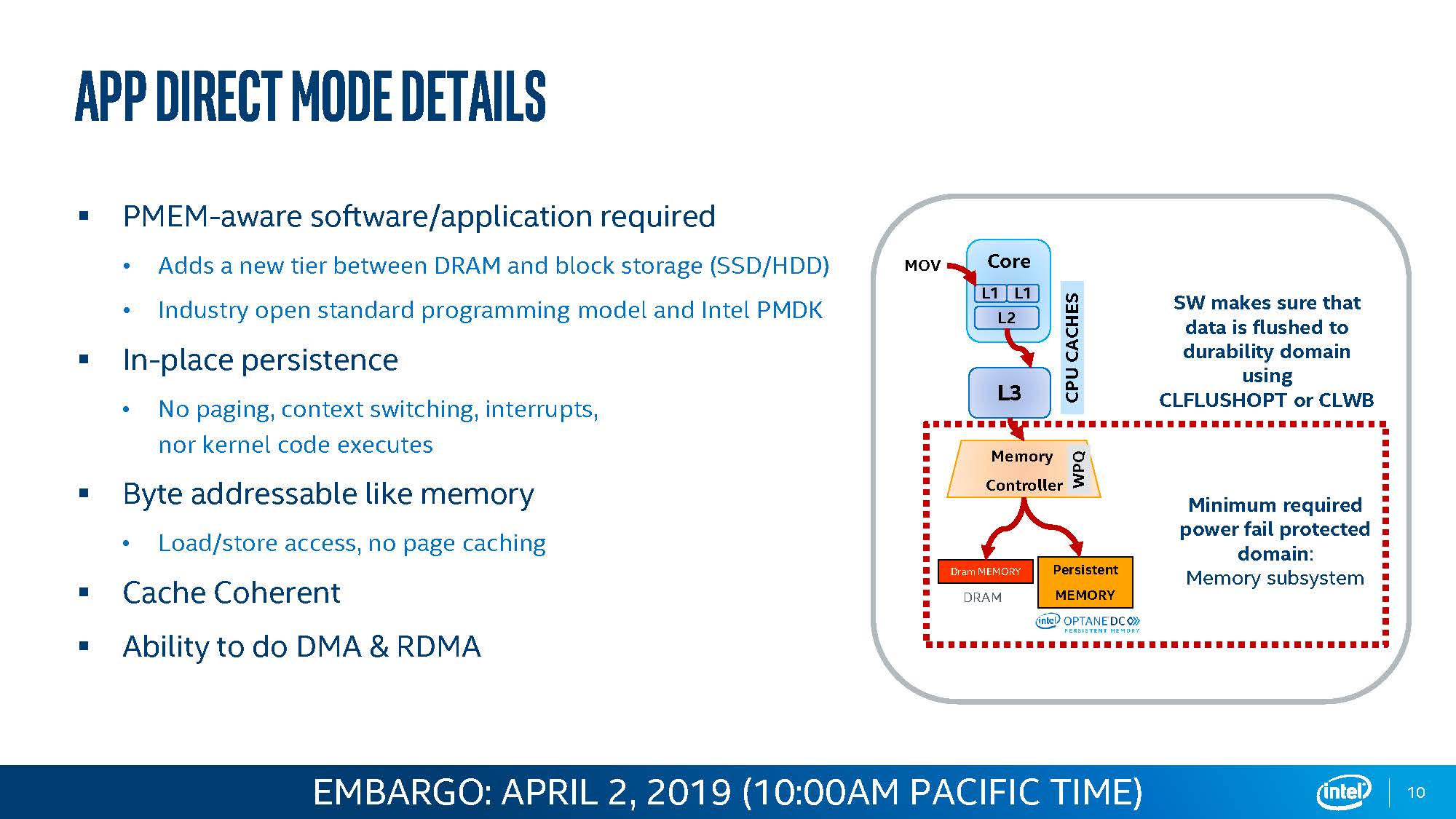
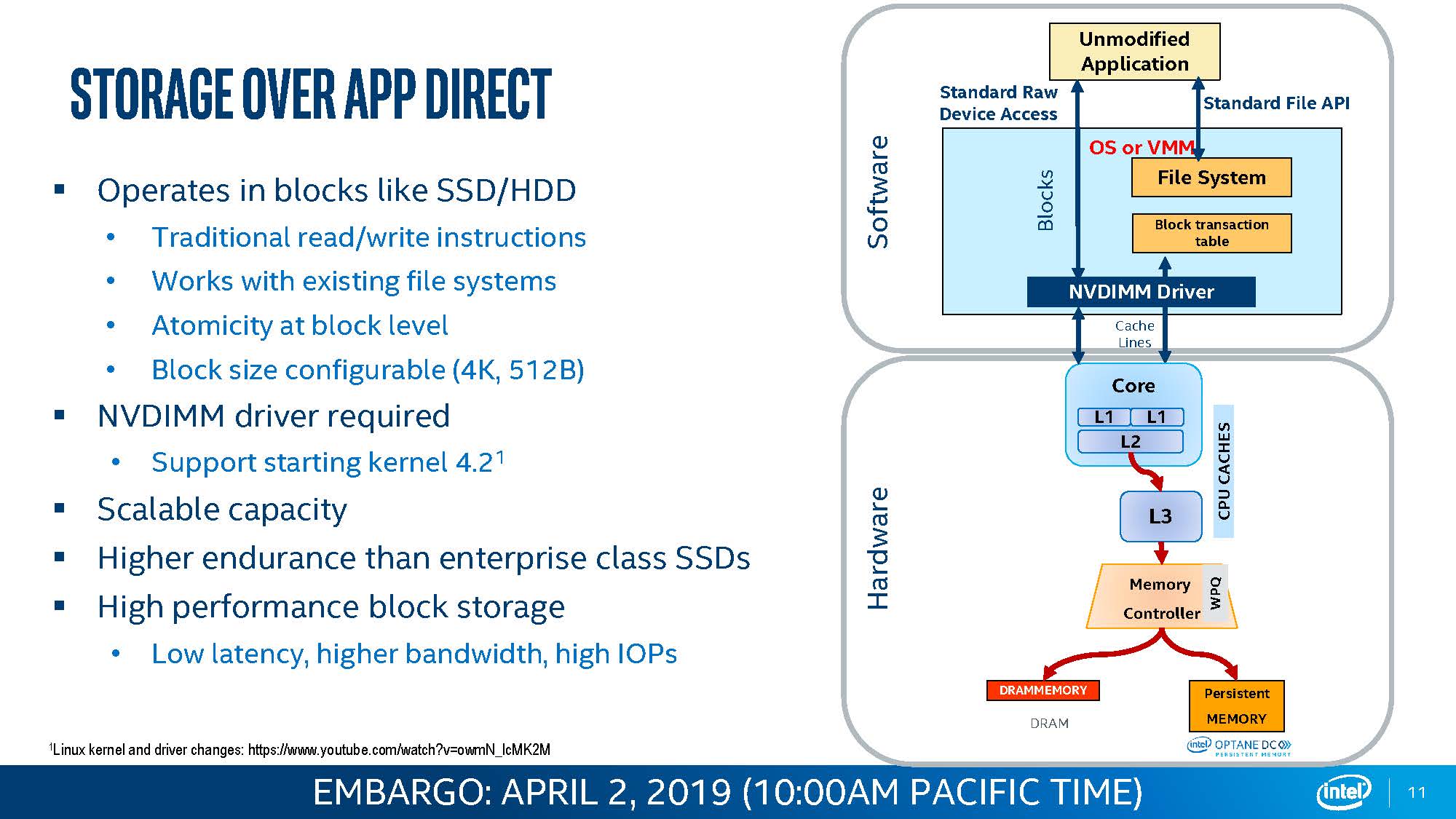
When one starts Optane PMem modules and wants to expose them as a normal block device in Storage Mode, it is actually quite analogous to a SSD. Each CPU has its DCPMM/ PMem Set of modules. The modules in each Set can be grouped into Regions. Namespaces can then be created either through CLI tools or usually, there are BIOS settings to do this. Those namespaces can then be exposed to the OS as block devices but there is another option for direct access (DAX) in some OSes that bypasses the traditional block set. You can look up terms such as ndctl and fsdax/ devdax for a bit more on this as the documentation is fairly good and those search terms will get you started.
The tricky part is that there is another layer of complexity that does not get discussed often. That is how you create the regions and namespaces. Optane for App Direct is roughly organized into a hierarchy:
- Set – this is a “set” of DCPMM/ PMem modules that sit on a CPU socket
- Region – definable grouping across one or more Optane modules
- Namespace – this is similar to a NVMe SSD namespace, but sits atop a region and allows one to define storage to transact on
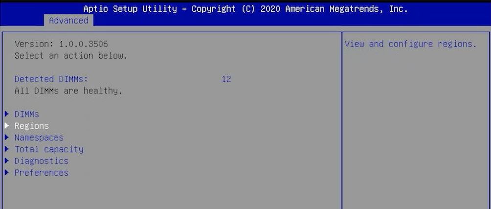
Your options are basically that you can use individual PMem modules or you can interleave them into a region. If you interleave the modules, it is like creating a large RAID 0 array of Optane P4800X/ P5800X SSDs. That is again a bit simplified, but the challenge is that data is written across modules to gain performance like a RAID 0 array. If one fails, then you lose data.
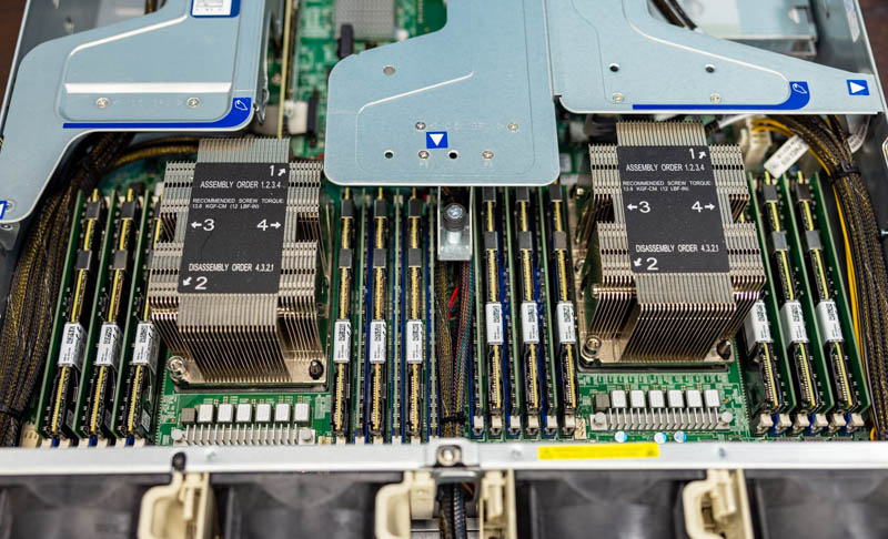
To counteract this, there is another option. One can expose a PMem module as its own region/ namespace/ block device. Then do things such as create RAID 1 arrays with them as if they were SSDs which gets in-system redundancy. Of course, doing this has a performance penalty versus the persistent interleaving modes. Also, if one mirrors across sockets, then that has to traverse the UPI links adding to latency until it is complete.
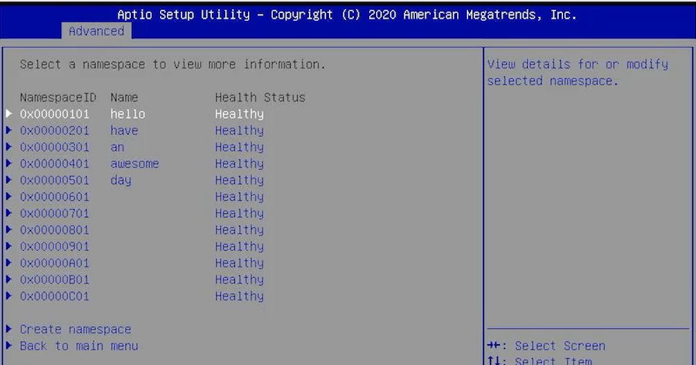
So the challenge is that to keep the module fast, we would want to interleave using a region across a CPU’s Set of PMem modules. Then, we are at risk of losing data so we then need to go to a lower performance state to get redundancy within a system. We can mirror data and transactions across a network to other systems, but that is another layer of complexity especially at the speed of Optane DIMMs.
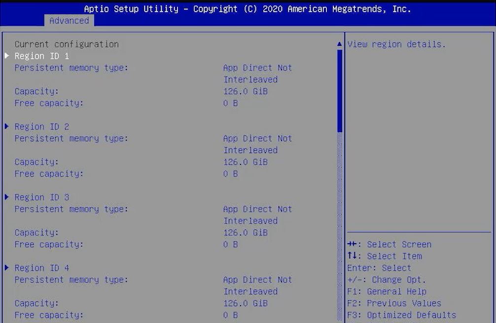
In App Direct/ Storage Mode, the DRAM functions as normal DRAM, and we get fairly pure access to the Optane DIMMs. Our capacity is close to the Optane DIMM capacity as persistent storage (App Direct) and memory which is close to the DRAM capacity in the system. There are overheads, but that is the conceptual model you can use. Then, things get more complex.
Glorious Complexity: Mixed Mode
There is one other mode called “Mixed Mode.” This is exactly how it sounds and allows one to access all of the complexity of Memory Mode while also not missing out on the complexity of App Direct mode. In other words, you can do both, on the same system, at the same time. One can provision say a third of our capacity for App Direct/ Storage while the remaining two-thirds are used for Memory Mode. In our 12x 16GB + 12x 128GB DCPMM example, we would then have around 0.5TB per socket reserved for Memory Mode for around a 5:1 DRAM to Optane ratio. The remaining 0.25TB per CPU can now be a set used to create regions and namespaces.
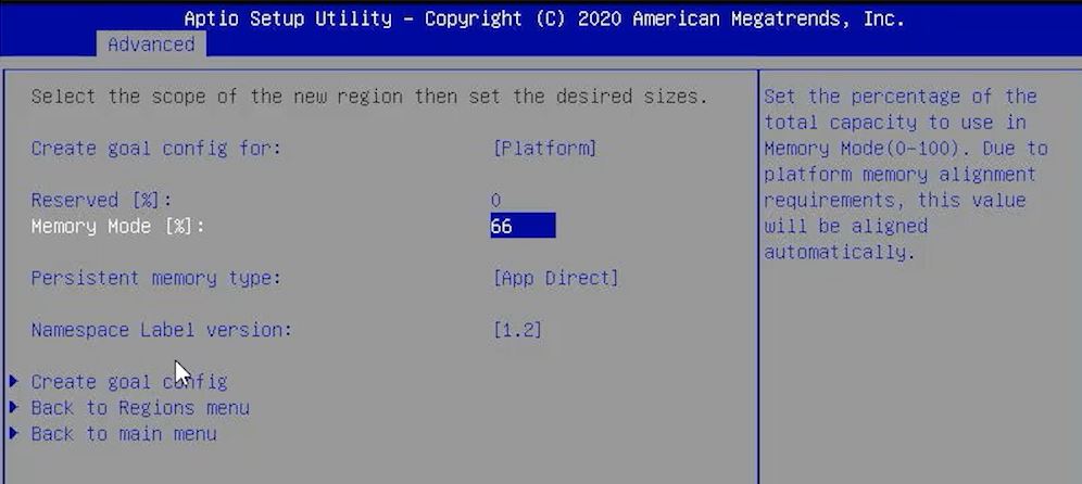
How one does this, is by setting a “slider” where one sets how much of the capacity is set aside for Memory Mode, with the remainder being set aside for App Direct use. Software determines how much goes to each pool and takes care of the alignment/ rounding. One will note here that we are showing this using Supermicro BIOS, but there are CLI tools that handle all of this and can do more granular controls (you can see “Create goal config for Platform” as an example.)
Mixed Mode is a cool feature, but now we are using the Optane DIMMs for the cold portion of main memory plus the storage so there can be a performance impact. The first application where we used this was to carve out ZIL/ SLOG space which had a small capacity impact but meant we could have another drive free and get the benefits of a fast ZIL/ SLOG device. Since that has modest capacity requirements, it not only freed a drive bay but also saved us from having to spend hundreds of dollars per machine to get drives like the Intel Optane DC P4801X 100GB U.2 NVMe SSD Log Option. We have found that Optane, in general, is an awesome SLOG/ ZIL solution for those running ZFS arrays.
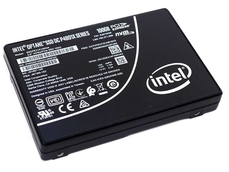
Sure it is complex, but it is also extremely useful. Using Mixed Mode to add mirrored write cache devices while simultaneously getting lower-cost memory expansion is immensely powerful, leading to our statement around “glorious complexity.”
With that background, let us get to the Micron announcement where they are discontinuing the 3D XPoint program.

You’re slow on the Micron announcement coverage. I thought STH was going to skip. Then this comes out. I’m OK if you’re slow but you get to this depth.
I learned, many of the teachings.
Not surprised that Micron exited – I would imagine Intel is the logical buyer for the facilities – and Intel does have its own 3DXpoint production line.
What Micron’s exit does is completely quell the talk about AMD using the Micron supplied NVDIMMs in its servers. But with the ultra low volume of Epycs installed – would likely have only covered the coffee and donuts in the break rooms.
With Intel moving its NAND lines to SKHynix, looks like the former Micron fab would make sense
3D Xpoint is #1 memory for make benefit ZFS SLOG. Very nice, I like!
I thought the title was Borat too. Very nice wifiholic.
Did anyone see the namespaces screenshot. It’s Patricks “Have an awesome day” sign off line. I was like “oh-no-you-didn’t” home skillet.
Great article.
Instead of doing all this newsi stuff, I’d like Patrick to just explain complex tech like this.
Oh and Bob D – you’ve embarassed yourself enough here. Move on. You’re the one who said STH only gets old stuff. There’s dcpmm 200 here. They did cooper. Zeeeeeeeeeeeero credibility.
Here’s one bit of complexity.
Unlike the DRAM, the xpt has a write failure rate nowhere close to 100%. It tries to hide this by reading after the write and redoing the failures… Which is almost transparent to the programmer except when sometimes an operation takes a few 100s more cycles than it usually takes.
For interactive parallelism is concerned and the question is “Y Slow?” it is usually that when you break work into N chunks, you have to wait for the longest N chunk to finish and that is not like averaging where increasing N evens things out, instead the variation gets more violent as N increases. When N>64 you have moved past simple load balancing and profiling has fixed the worst problems, further scaling is a “search-and-destroy” mission for exceptional events of that type.
Also if an operation gets delayed there is more time for something to happen with other threads, you might miss the happy path for lock elision and now it is 10,000 cycles, etc.
Thinking as a high-performance programmer xpt doesn’t feel like DRAM to me. As a low performance programmer who uses 1 Python lambda function to turn on a light bulb it does.
Speaking of threads, what happens to the memory controller and cache system when an optane write is stuck? Is everything else running on all cylinders? Or could other memory transactions (for instance to to the same Optane stick, or to another Optane, or a DRAM) get delayed?
Intel seems to have basically gotten the math right for the memory controller but what opportunities were missed along the way? Would Intel have served customers better if it was focused 100% on DRAM?
xpt always seemed to be from another planet where you have a tablet with 32 GB xpt and an e-ink screen; it is like the ATMEL program memory cell that made the AVR8 a legend and it ought to be taking computers to “where none have gone before” instead of trying really hard to outcompete two world-beating technologies at the same time.
I mean, odds are Intel will just… buy Micron’s factory, no? They just committed to doing more die manufacturing in-country, it’s a no-brainer
Thank you STH / Patrick for this article!
As an old computer sciences professor said: “Computing is the science/art of moving bytes.” The rest is just more explanations.
3D XPoint is #1 memory to make ultimate storage system DAOS, actually…
Andrew, I would have presumed that the SKHynix deal would have involved targeting their fans for future production?
fabs obviously typo sorry
domih
it’s in Knuth TAOCP there is nothing in computing unintelligible to a railroad sidings master and turntable.
I paraphrase but that’s essentially it
of course nothing stops OPTANE / 3DXP turning up with a CXL or other serial interface, or being integrated by server manufacturers to buffer gpu memory..
it belatedly occurs to me that OPTANE may be on life support because of government and military supply contracts which require long commitment and the cost of support possibly including very long life sku resupply together with the very quiet position of micron throughout this history could be explained by legal necessity of dual source
You really love your Optane but you don’t really do research on mem business:
1. Going back to IMFT it was Micron that did almost all of the R&D for both NAND and 3DXpoint and Intel paid Micron handsomely on a querterly base. Look at the 10-k and 10-q of that time. Intel has very little memory R&D.
2. “Micron’s announcement doesn’t change our strategy for Intel Optane or our ability to supply Intel Optane products to our customers”
That’s the same stuff they said aout NAND when IMFT split but Intel did no further development. Intel remained on floating gate tech and the only thing they did was to add another stack on top to get to 144L (even that was probably Micron#s development but they opted for the move to charge trap).
Then they sold all their NAND cabs and controller tech to Hynix but they are still not allowed to sell the technology that Micron developed so the actual transaction for the NAND fabrication and IP has to wait until March 2025.
3. Intel is most definitely not buying the Lehi Fab from Micron.
It is very unlikely that Micron would make such an announcement when they were expecting a sale to Intel. They would have waited until they could just say that they sold all of 3DXpoint to Intel.
Micron has also moved out a lot of tools to other (DRAM) fabs due to “underutlization”. It was announced during an earnings call not to long ago. If Intel showed interest in buying this fab micron would have kept all tools there and sold it as a 3DXPoint fab.
4. You’re comparisons to “todays” QLC-NAND are just weird. If any competitor would see a market for it they could very easily develop SLC NAND chips with very short string lengths (z-nand and xl-flash did that partially). These chips would be much more expensive than todays standard TLC/QLC chips but they would still be much cheaper than Optane. Micron is seeing that cost problem (paragraph “on the storage front”) but you are not. Optane has no place in storage.
5. Power-loss protection for SSDs is not considered a challenge to anyone and it’s absolute standard and working fine.
“ That ratio is a big challenge though. For example, if one wants to use 128GB DIMMs with a 4:1 ratio, then one needs to populate a 32GB RDIMM and a 128GB PMem module in the same memory channel.”
I remember Intel taking a stab at using octane caches with slower storage devices(after a similar attempt at using NAND caches with HDDs, both seem to have sunk into obscurity fairly quickly): is there, or has anyone proposed, an option that moves the optane right onto the same DIMM as the DRAM it is serving as a cache for in order to reduce the complexity of populating the memory channels? Or is that simply not supported by the memory controller and/or a nightmare of SKU proliferation since the desired DRAM/Optane ratio is now baked into the DIMM rather than being configurable by purchasing a selection of DIMMs to suit?
Aside from all that, the optane application that seems like it could be really cool is in very low power/often sleeping applications.
If you take a nonvolatile RAM-like and move it all the way in to the CPU or MCU: cache, registers, everything; not just RAM, you get a device that no longer need have a distinct sleep/wake cycle or a boot process(except for the first time or if you need to flush problematic state and start fresh): if you have enough power to execute at least one instruction to completion you run, otherwise you stop.
“CXL is not a replacement for 3D XPoint”
CXL can very well be a replacement for 3DXPoint: CXL allows large amounts of DRAM (dozens of TB) to be accessed fast and with low latency. DRAM capacity won’t be limited by channels and ranks anymore.
In general I think you are overstating then benefits of Optane persistency in in-memory-DB applications as most real-world DB usages don’t have enough writes/merges to be limited by stores/logs on SSDs.
SAP HANA runs just fine on DRAM/SSD combos and Optane is barely used. It’s mostly used when additional DRAM capacity gets extremely expensive (2DS 256GB DIMMS) or that capacity is impossible to achieve with DIMMs. CXL could really help with more linear DRAM capacity-cost.
Lasertoe – CXL is like a transport link. 3D XPoint is a type of media.
@Patrick “Lasertoe – CXL is like a transport link. 3D XPoint is a type of media.”
Yes it is a transport link. CXL.mem protocol (coherent) and CXL/PCIE5.0 to DDR4/DDR5 controllers with lots of DIMMs can replace 3DXPoint for many applications (seems to me that Micron is working on something just like that):
You can have much more DRAM connected to your CPU this way. Example:
Instead of just having 8 DDR-channels connected to DIMMs you can have 8 or 16 CXL links connected to mem controllers with 8 DDR-channels each. That will allow a multiple of the DRAM capacity that is possible today.
That will eliminate any capacity advantage of Optane. It will just be about DRAM cost and whether (full) persitency is really necessary or not.
Bob Dobbs, Intel does not have its own 3D X-Point production line. The only production line is Micron’s.
A useful writeup on the tech, though anyone interested in the tech could have found most of this out a while ago, just nice to see it all in a Google searchable article.
Optane for ZIL/Slog is not a game-changer for the industry which on the whole doesn’t even consider ZFS a key storage layer in any respectable high-end stack; what the kids play with doesn’t bring home the golden eggs I’m afraid.
However this will inevitably flood the market with remaining Optane stock at affordable prices, we’re already seeing the trend over in the chinese B2B segment. That is a positive for the aforementioned kids.
CXL is most definitely the way forward. Micron made a wise decision, to be frank I’m surprised they held-on as long as they did.
Will be interesting to see where Intel go next, they’re losing ground and direction across most sectors currently.
Intel needs to stick to a segment rather than giving up every time it feels a little pressure.
Optane has a lot of potential. It needs time to grow, and they need to work not only on getting it work with all their Xeons, but work more like regular DDR so it can be used on AMD and ARM systems that are willing to support it.
The P5800X with it’s second generation 3D XPoint improves sequential read/write performance by 3x. If we get the same with “Crow Pass” 3rd Gen Optane PM DIMMs, we’ll have 20GB/s read and 10GB/s writes, and also get the latency even lower.
They said 3rd Gen DIMMs are an Inflection Point so we’ll see in what area it evolves in. I really hope it moves to fully open it up.
You know how big companies with acquisitions always claiming they’ll treat the acquisitions as a separate entity? They almost always don’t and the main company meddles too much in it causing it to fail.
Is it possible to use Pmem 200 with 2nd Gen? then you would at least be able to run 2933 as designed?