At NVIDIA GTC China 2020, the NVIDIA showed off a number of advancements. We wanted to highlight two big themes from Bill Dally, NVIDIA’s Chief Data Scientist and SVP of Research’s keynote. Those two key themes are co-packaged optics and AI inference which are designed to scale-up and scale-out the company’s reach with its compute capabilities.
NVIDIA Co-Packaged Silicon Photonics
During Bill’s keynote, he touched upon key themes we have been covering for some time at STH, silicon photonics and co-packaged optics. Transmitting bits over distance has some energy cost. That energy cost generally increases based on speed and distance. Current electrical interconnects, as we see in the NVIDIA DGX and a HGX platform we reviewed in the Inspur NF5488M5 Review A Unique 8x NVIDIA Tesla V100 Server, are running at around 8pJ/b with 25Gbps per link signaling while being limited to 0.3m or around 1ft. A consequence of this is that high-speed topologies are limited to in-box designs and quickly require switches like NVSwitch and retimers to span longer distances that are still relatively short. While this keynote focused on NVLink, PCIe will see this soon which will require changes after PCIe Gen5 (although when is up for debate) to reach rack-scale disaggregated computing. NVIDIA is showing an industry challenge here.
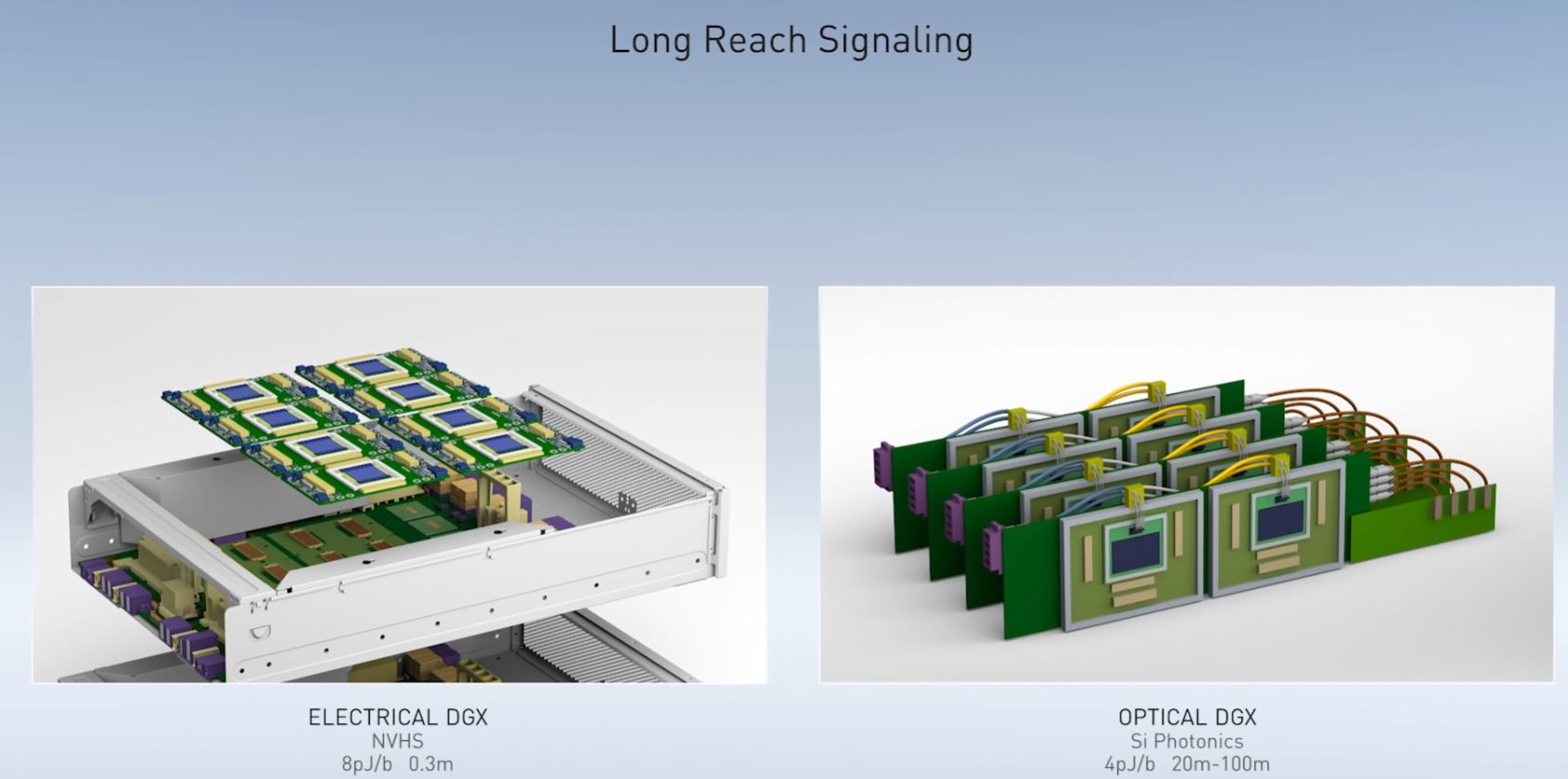
“The way we plan to do this is with a relatively new optical technology, Dense Wavelength Division Multiplexing.” (DWDM) Bill Dally NVIDIA at GTC China 2020 Keynote.
DWDM has been used in networking for decades, but the basic idea is that a comb light source is used and different colors of light are used over a single fiber optic cable with each color being a distinct data path. Each color is modulated to encode data and then at the end of the link each color is detected separately. Instead of adding multiple electrical traces (wires) to scale-out bandwidth, DWDM can use more colors of light. NVIDIA discussed using 32 colors, but 128 lane DWDM even for long haul communications have been around for 10-20 years. That means from a 32-lane design, there is a well-known path to scale both transmission speeds per color, but also the number of colors used to increase bandwidth well into the Tbps era.
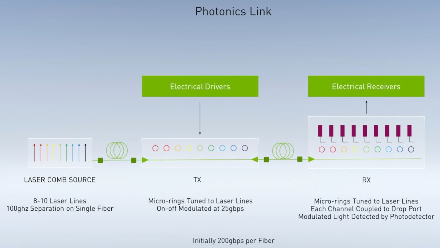
Switching to optics lowers the power required to move data and provides high signal integrity over long distances which will become more important as the company needs to increase the bandwidth through processors.
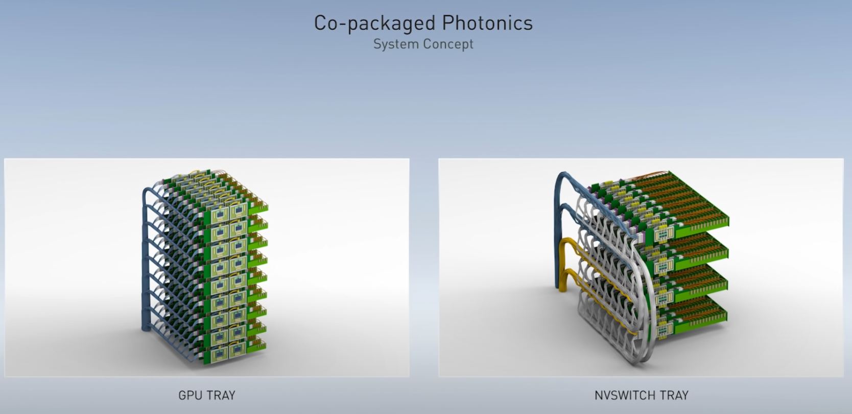
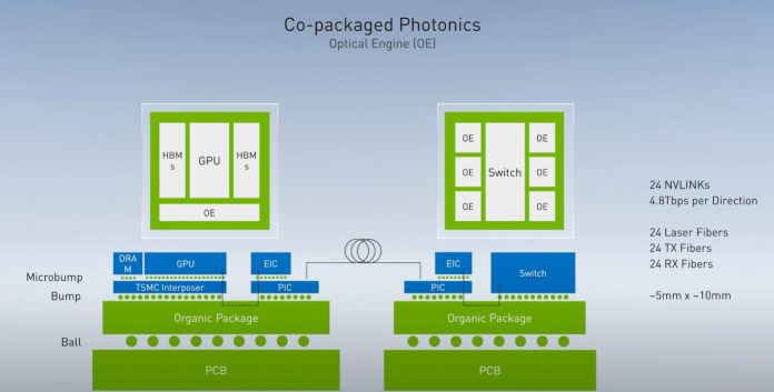
NVIDIA showed off a design for co-packaged optics both with GPUs, on the GPU package, as well as with switches for 4.8Tbps NVLink. To put that in perspective, 4.8Tbps is faster than many of today’s CPUs can ingest data through memory hierarchies.

With photonics replacing electrical signaling, NVIDIA can scale-up systems in a more disaggregated fashion. No longer is a system limited by 0.3m electrical traces which means more devices can be aggregated to different topologies. While these examples are focused more on the DGX-style of computing, next-gen NVIDIA BlueField is another prime candidate for integrating optics instead of using pluggable modules at some point in the future.
NVIDIA still has some way to go. Not only will the company need to move to co-packaged optics for GPUs, at some point its networking division, spearheaded by the Mellanox acquisition, will need to adopt co-packaged optics as well. We asked during the recent NVIDIA Mellanox NDR 400Gbps InfiniBand announcement and while DACs were still possible, there is a recognition that co-packaged optics needs to happen. At STH, this is something we have been following for some time. We even had exclusive hands-on access to Intel’s co-packaged silicon photonics demo earlier in 2020.
We hope that NVIDIA is further along in its photonics journey than described in the presentation since that is going to be a major enabler of architecture in a few generations. The network switch players are at the point they are telling us it will be the amount of adoption rather than if there will be adoption at the next 51.2T generation with an eventual industry transition. Those 51.2T switches are on roadmaps and not far off. Even if not for its GPU side, NVIDIA will need this for the network fabric side earlier, but it would be great to see NVIDIA have future GPUs have this for a “killer app”.
AI Inference and Efficiency
On that efficiency theme, NVIDIA also discussed inference performance. As some context, Chinese AI researchers are moving quickly into the realm of putting AI models to practical applications, something we discussed recently in AI in 2020 and a Glimpse of 2021 with Inspur and NVIDIA. NVIDIA for its part is showing its inference performance scaling to meet the challenge of this rapidly growing workload.
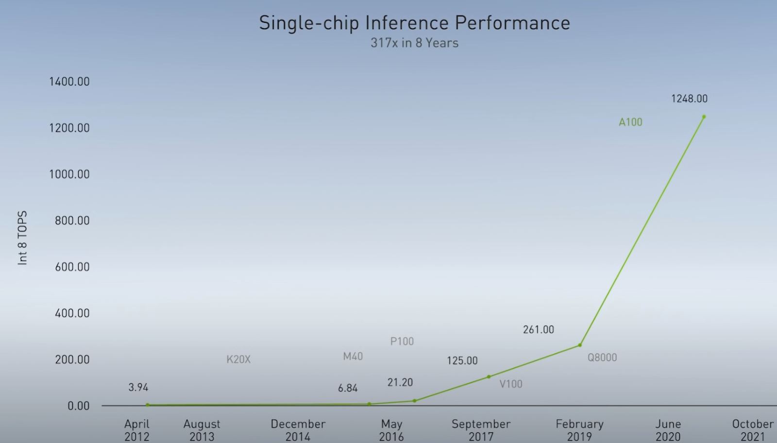
Part of the discussion was broader around dedicated AI accelerators such as the Intel Habana Labs offerings that Facebook selected over NVIDIA GPUs and Amazon AWS recently announced EC2 Intel Habana Gaudi Instances as examples, but other smaller players are in the market as well. Here, NVIDIA is showing its specialized instructions reduce overheads of data movement. In turn, the computations occur with less overhead while maintaining GPU programmability and flexibility.
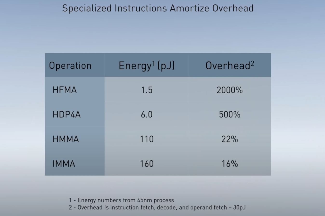
Specifically, on the inference side, NVIDIA showed off its RC18 or research chip 2018 that it previously published on at 9 TOPS/W. It then showed a next-gen at 29 TOPS/W.
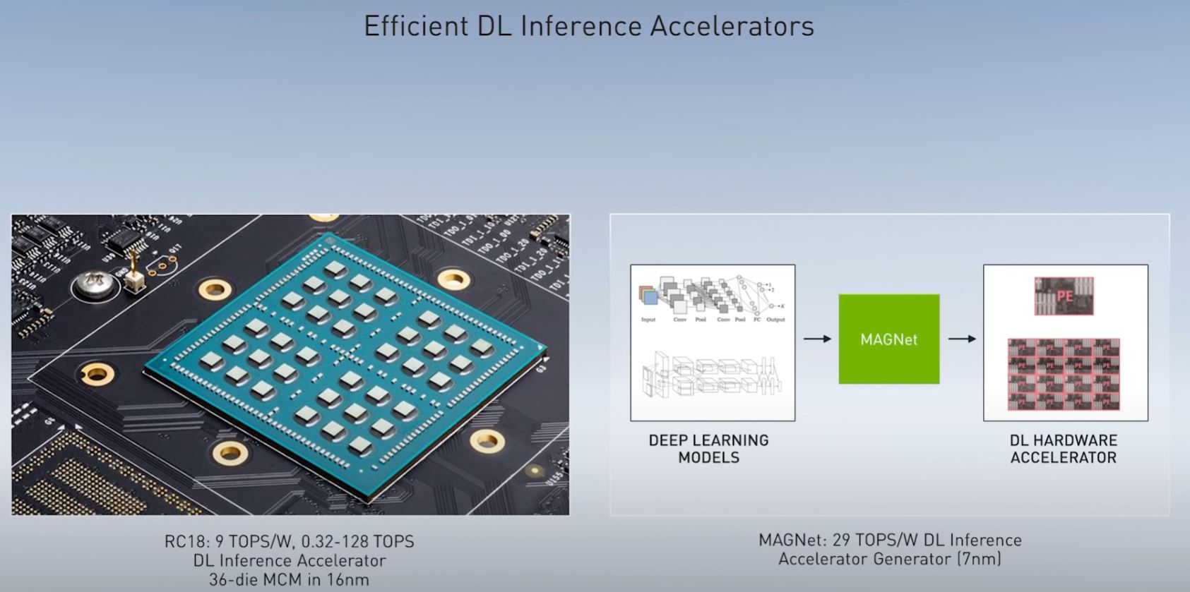
Much of this has to do with a more-optimized data flow to maximize the power/ performance of each operation. For inference to become ubiquitous, it needs to be low power as many of the applications will use solar, battery, or other limited power sources and also produced in great quantities.
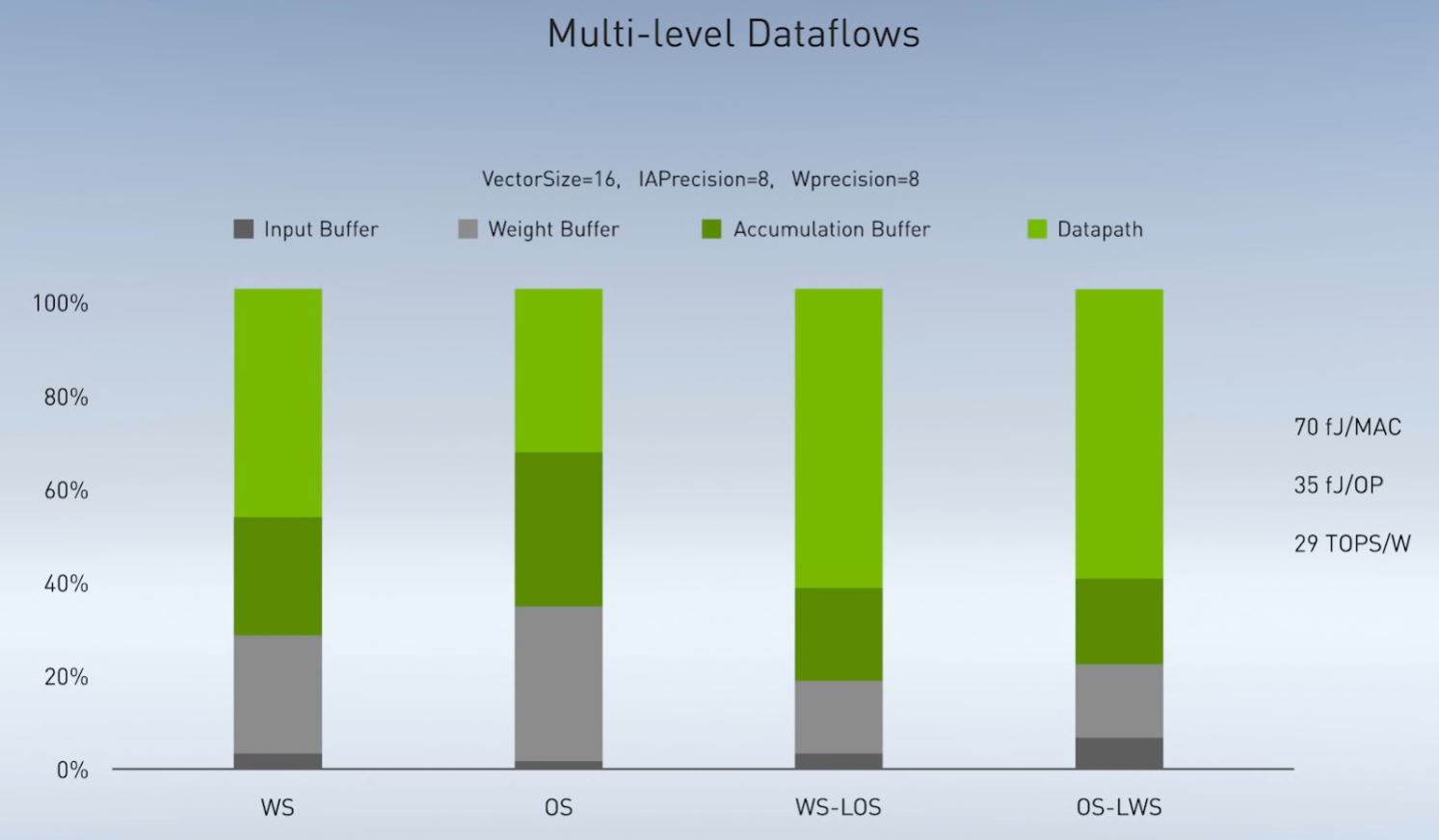
Another claim made during the keynote was that NVIDIA now has a test chip at 100TOPS/W. Although NVIDIA said it was not a commercial product, the implications are immense. With the pending NVIDIA-Arm acquisition, this is the type of NVIDIA IP that could potentially be added to the Arm licensing library in the future.
NVIDIA Orin and The Product Not Named: Jetson Ampere
Along the key theme of inferencing, there are a number of Chinese companies working on autonomous transportation projects. As such, NVIDIA is using GTC China 2020 to show off its next-gen autonomous vehicle platforms. For the show, the company showed off its next-gen autonomous vehicle chip, the NVIDIA Orin. Per NVIDIA:
“The Orin SoC integrates NVIDIA’s next-generation GPU architecture and Arm Hercules CPU cores, as well as new deep learning and computer vision accelerators that, in aggregate, deliver 200 trillion operations per second—nearly 7x the performance of NVIDIA’s previous generation Xavier SoC.” (Source: NVIDIA)
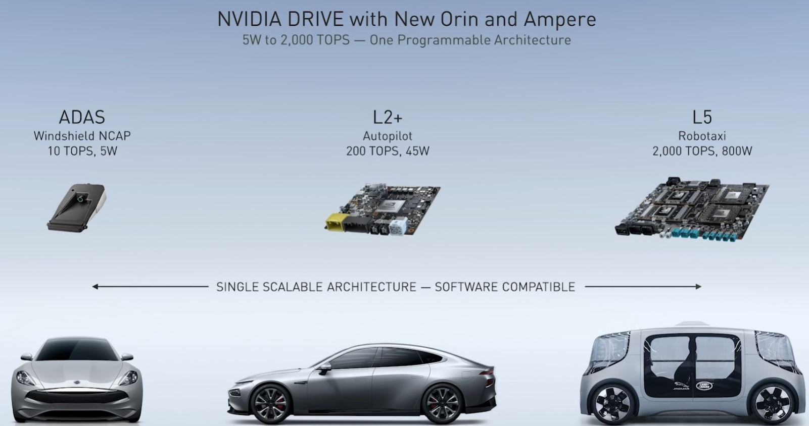
The L5 Robotaxi card is said to take two of these Orin SoCs along with two Ampere GPUs for redundancy. NVIDIA has been making hardware for autonomous vehicles for some time but says that this new platform is designed for the 2022 vehicle production timelines.
Earlier in the talk, Bill showed off an Ampere SXM module and said:
“We can scale the power that’s in Ampere from this module (SXM A100) for very demanding computing problems, all the way down to our Jetson line of products to our Jetson products.” Bill Dally NVIDIA at GTC China 2020 Keynote.
He gave this line while transitioning from a A100 to a Jetson module.

While the company did not announce a Jetson Ampere edition, it makes sense something like this may be coming. One can also see a Jetson box in the background next to a GeForce RTX 3090.
Final Words
Overall, we did not get a major new GPU announcement, and we stretched our hope beyond Orin to hoping this hints at an Ampere Jetson. Still, NVIDIA’s work on AI inference as well as co-packaged photonics show more than the focus on a particular GPU. Instead, these projects are designed to scale and proliferate AI. In the data center, co-packaged photonics will allow for larger and faster system topologies that will help scale-up and scale-out compute to tackle bigger challenges. For the edge, the AI inference efficiency, plus some of what NVIDIA has been showing in products and future compute elements shows how the company is planning to bring inference performance up and power consumption down to meet the needs of more applications. Short of a new GPU announcement, these are exciting visions for the future.



I first read about DWDM last century – am I missing something besides progress in packaging and the advances in silicon emitters?