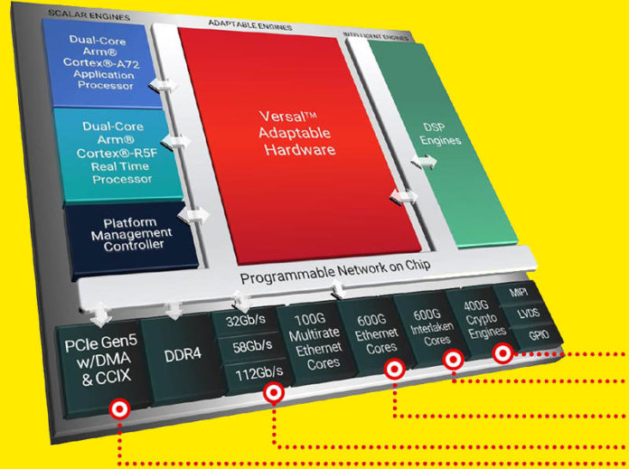
We previously covered the Xilinx Versal Premium, but Xilinx is releasing more information about the solution at Hot Chips 32 (2020.) We wanted to share some of the new details. Since this is being done live at a conference, we may follow-up with an additional piece later and update this piece as the conference goes on.
Xilinx Versal Premium Overview
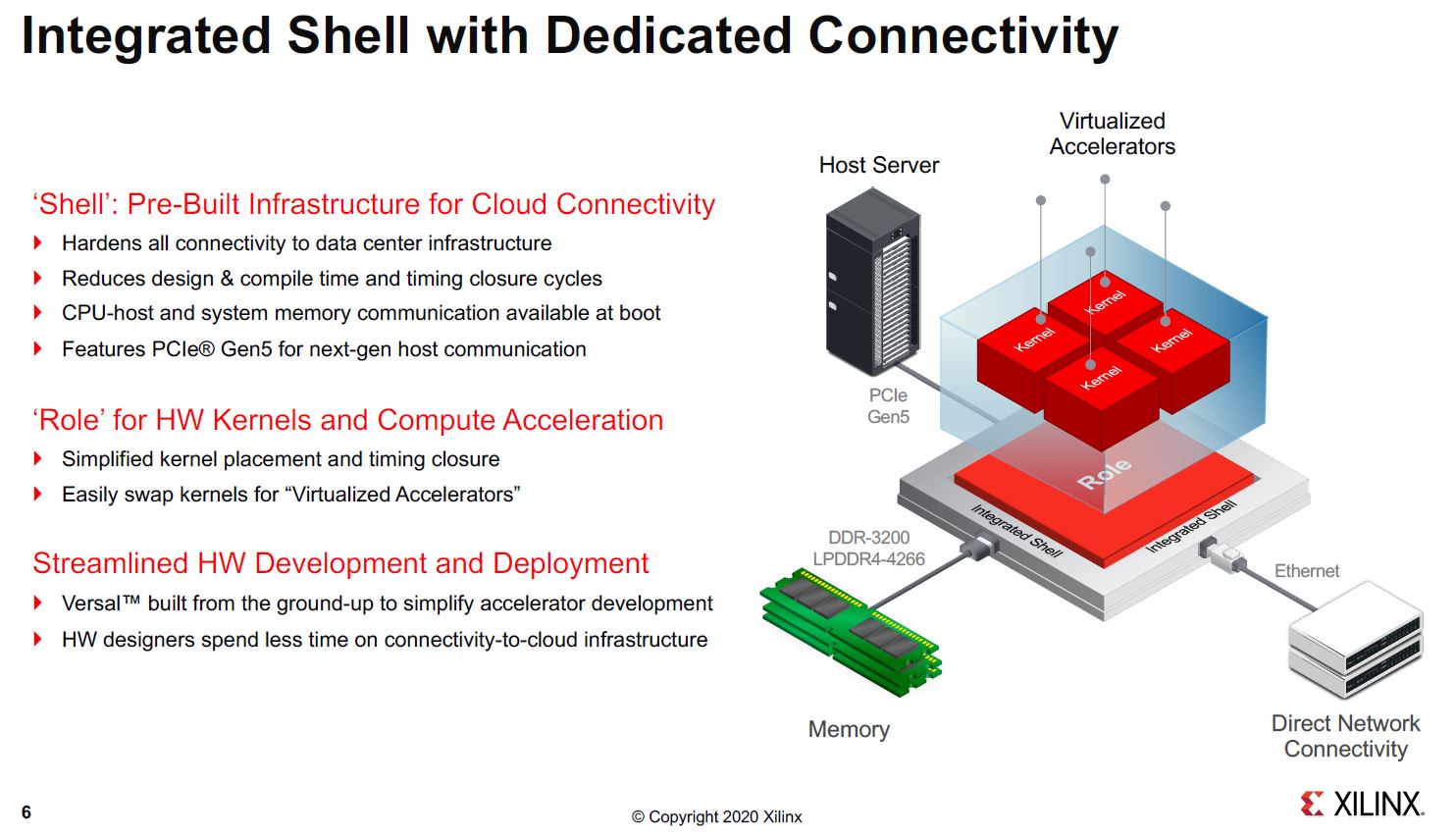
You can check out our Xilinx Versal Premium overview for more high-level information and how it works in the context of a 5G infrastructure build. One of the big features is the integrated shell which pre-builds a lot of functionality so that FPGA RTL programmers do not have to start from scratch to make Versal useful. This may not make sense at first, but it allows features such as PCIe and DDR interfaces to be available at boot instead of having to get that logic placed.
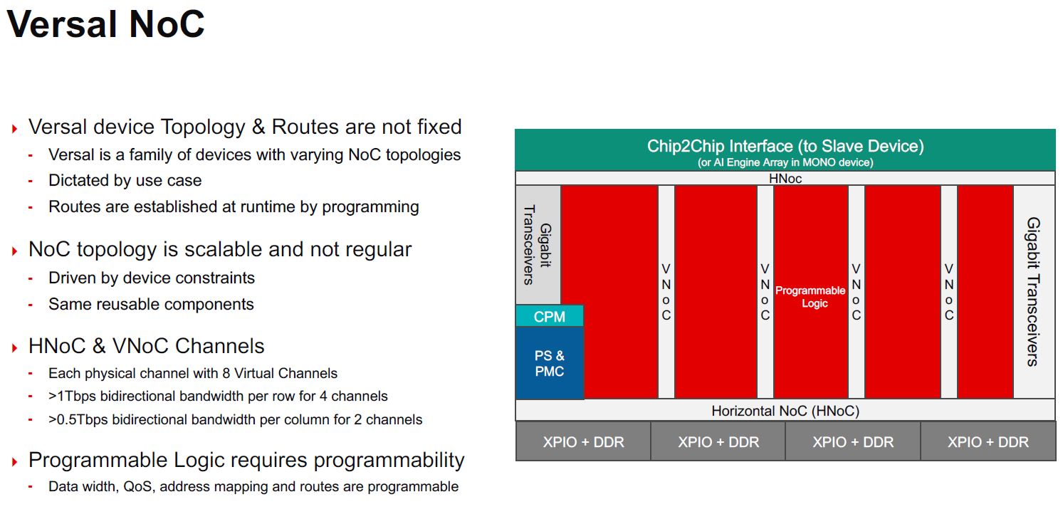
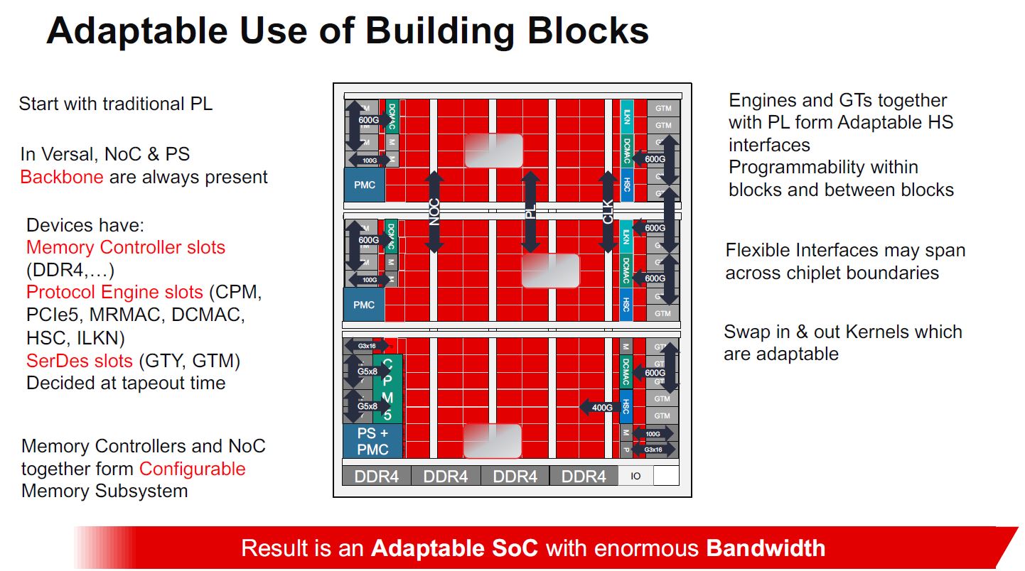
With all of the different logic blocks and I/O in the system, Xilinx is pushing its network-on-chip or NoC approach with features such as QoS.

Xilinx says that the Versal NoC is not completely fixed. As a result, it can be scalable and configurable for a given application and operates in the Tbps range.
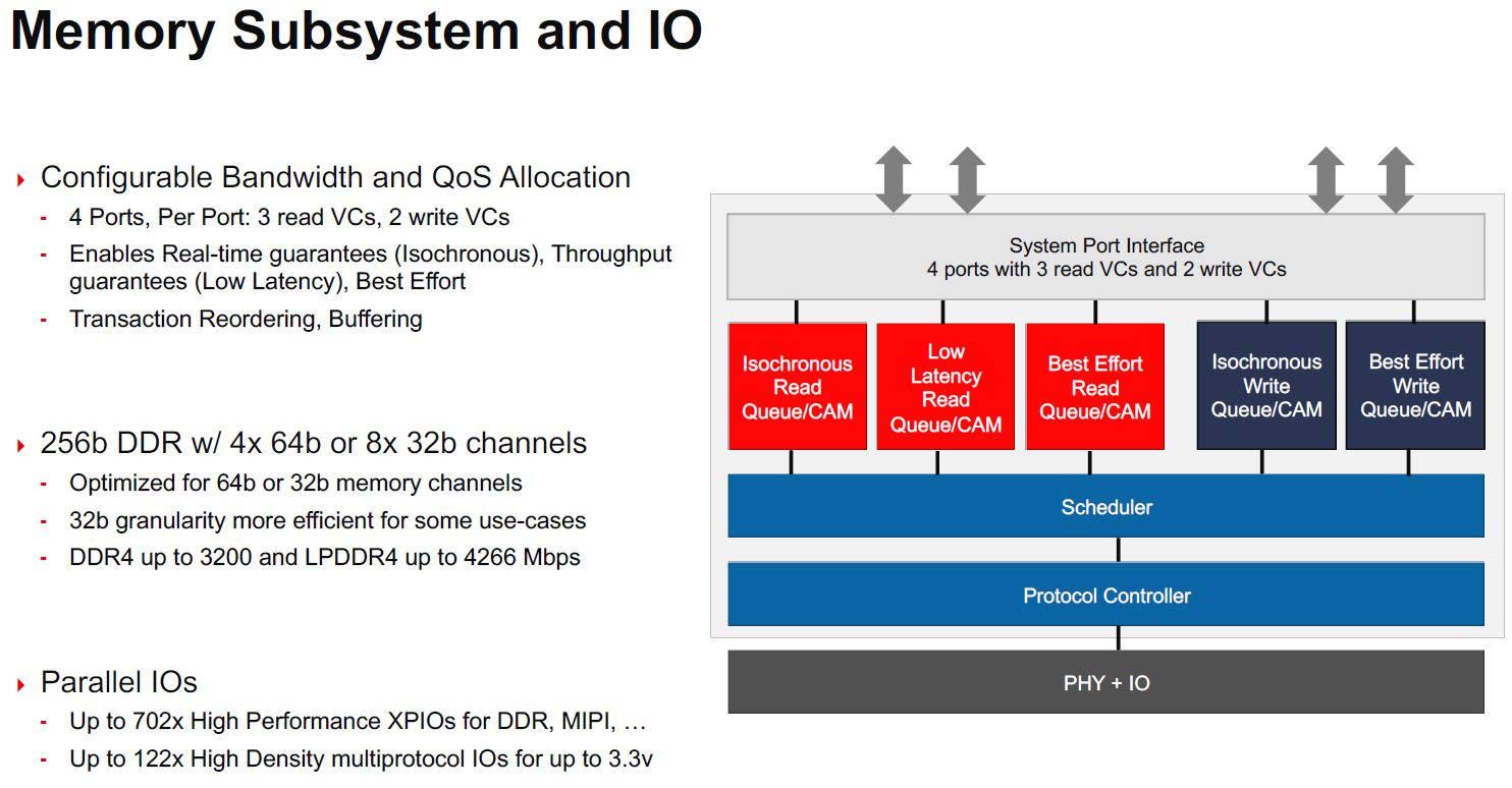
With the memory subsystem, the Versal Premium can work with DDR4 and LPDDR4 memory. There are, of course, other memory that Xilinx has access to.
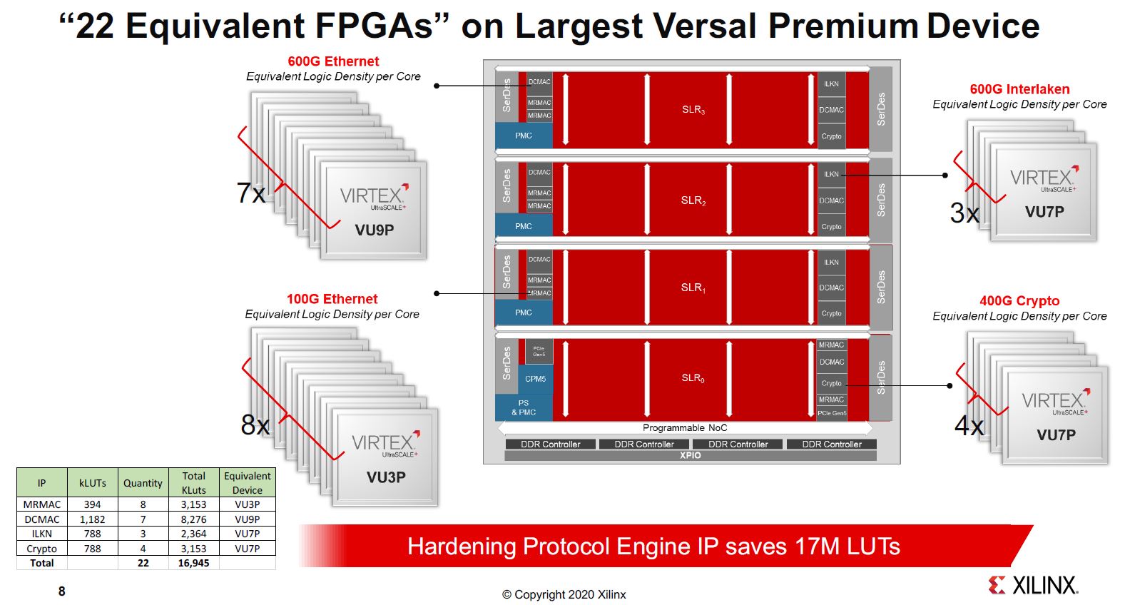
Xilinx says that the big Versal Premium is equivalent to 22 Virtex FPGAs due to its I/O and hardened Protocol Engine IP. This is just an interesting way to describe the product.
Let us get into some of the features.
Xilinx Versal Premium Features
While Intel Agilex is focused heavily on external tiles, Xilinx has a different way to conceptualize I/O and what should be hardened logic on the FPGA (or ACAP if we are still using that term.)
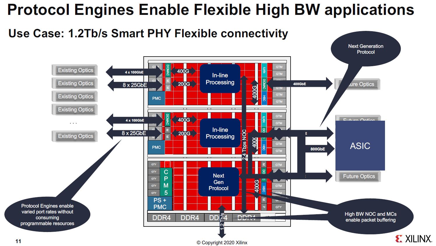
Xilinx has a huge focus on Versal Premium connectivity. For example, one can add features such as Ethernet and Interlaken as well as connectivity to custom ASIC integration. This example is building a 1.2Tbps smart PHY.
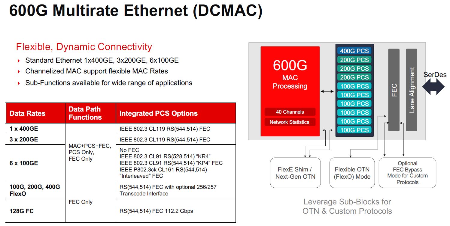
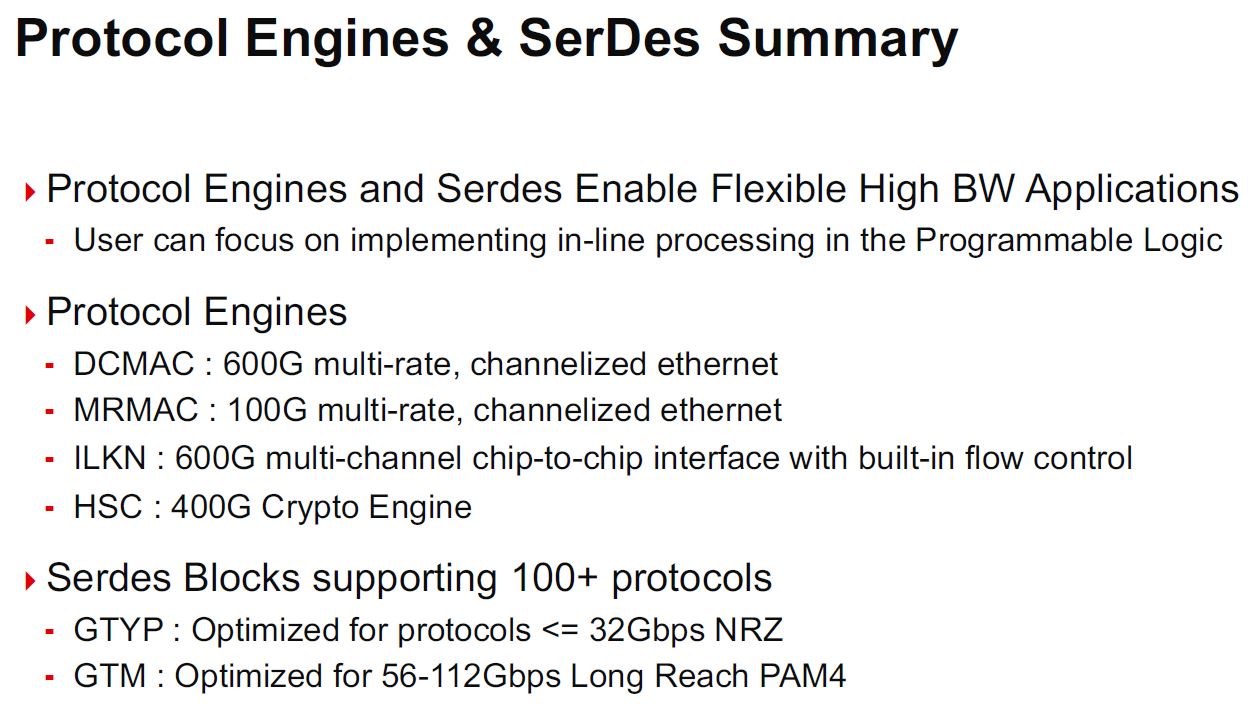
Some Versal Premium SKUs have 600G Multirate Ethernet or DCMAC. These can handle 6x 100GbE, 3x 200GbE, or 1x 400GbE.
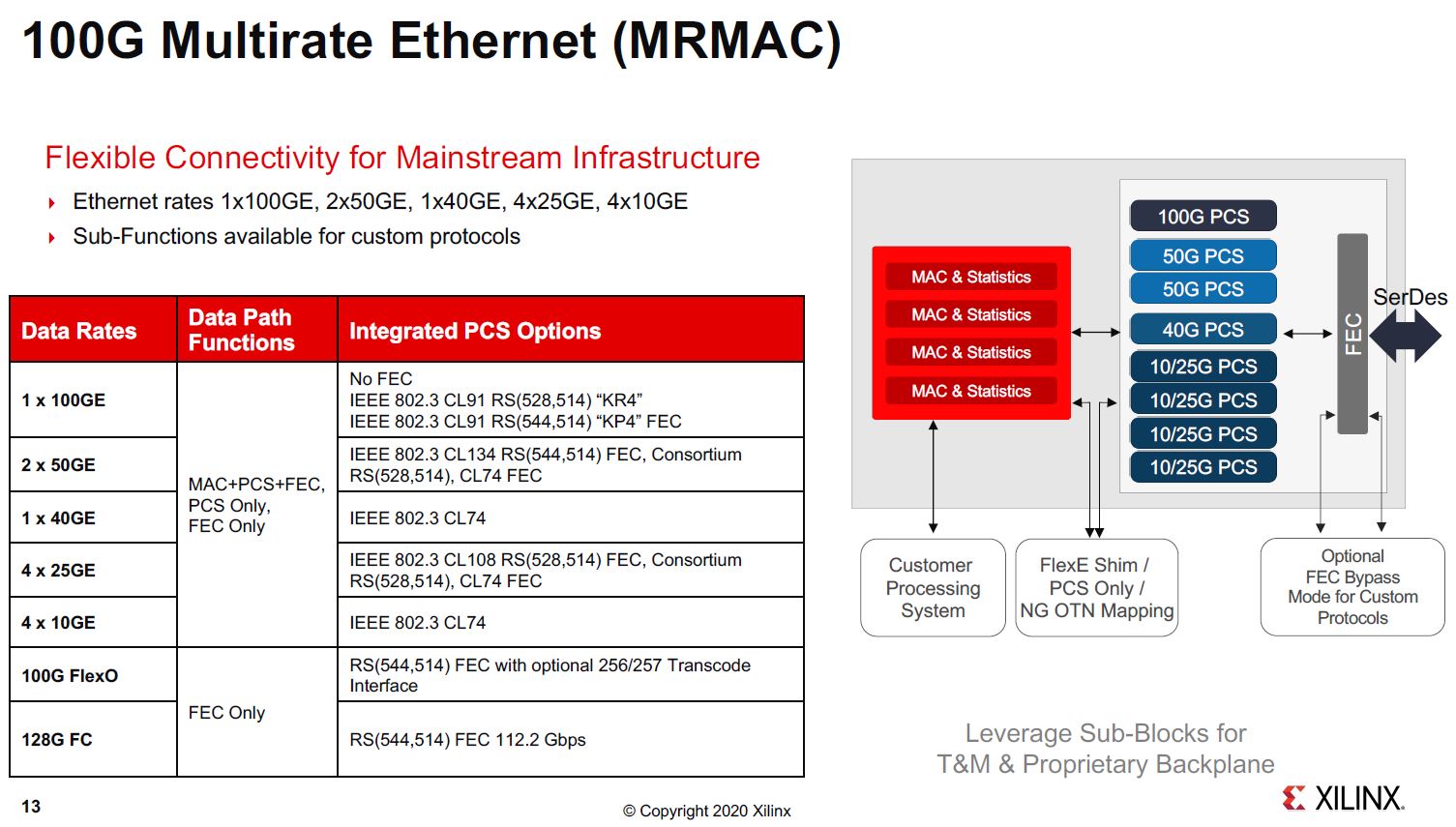
There is a lower-speed 100G Multirate Ethernet (MRMAC) option as well. This is what scales down to slower speeds such as 10GbE, 25GbE, and 50GbE.
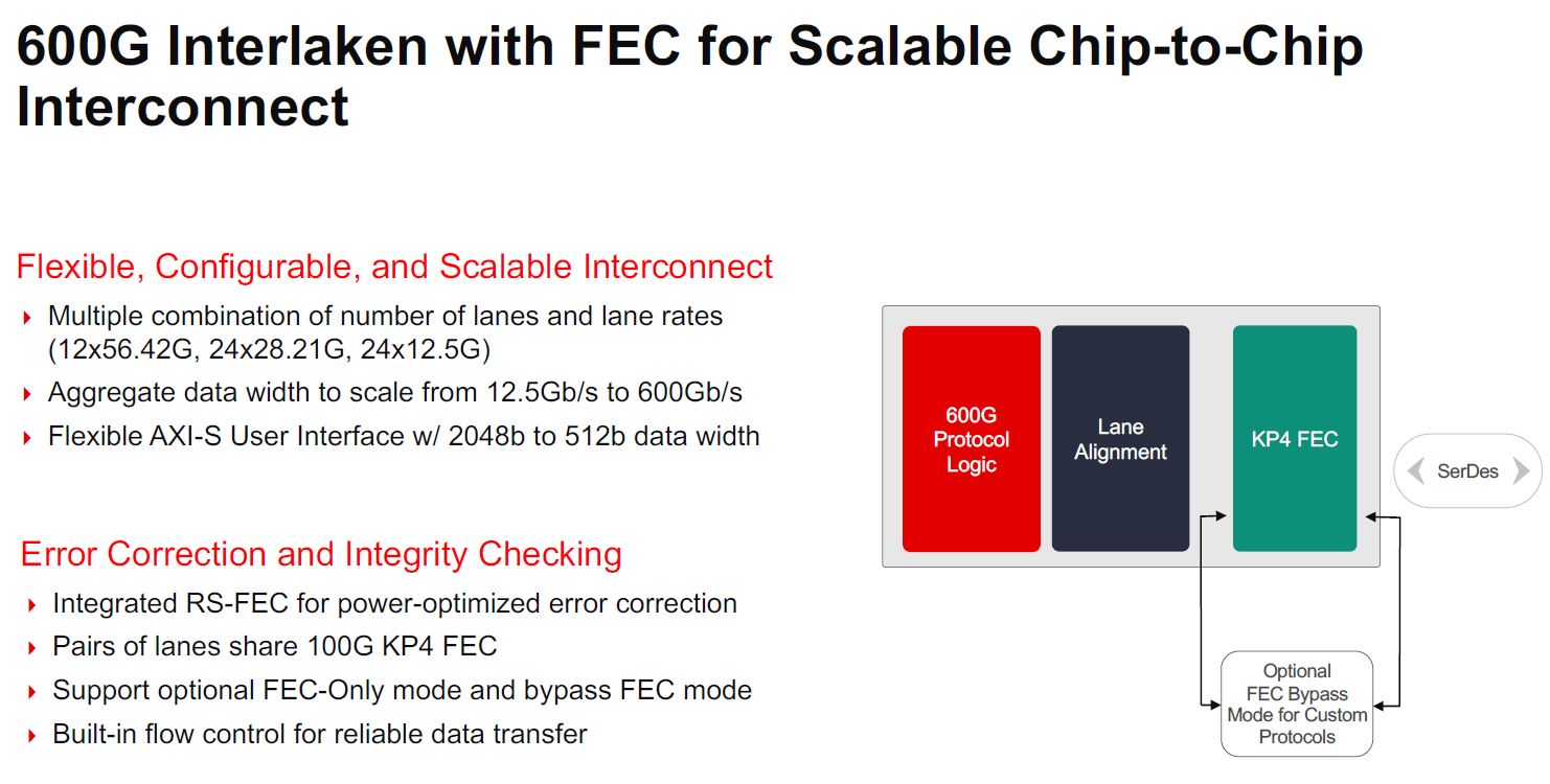
The 600G Interlaken is important for integrating the Verasal Premium into larger solutions.
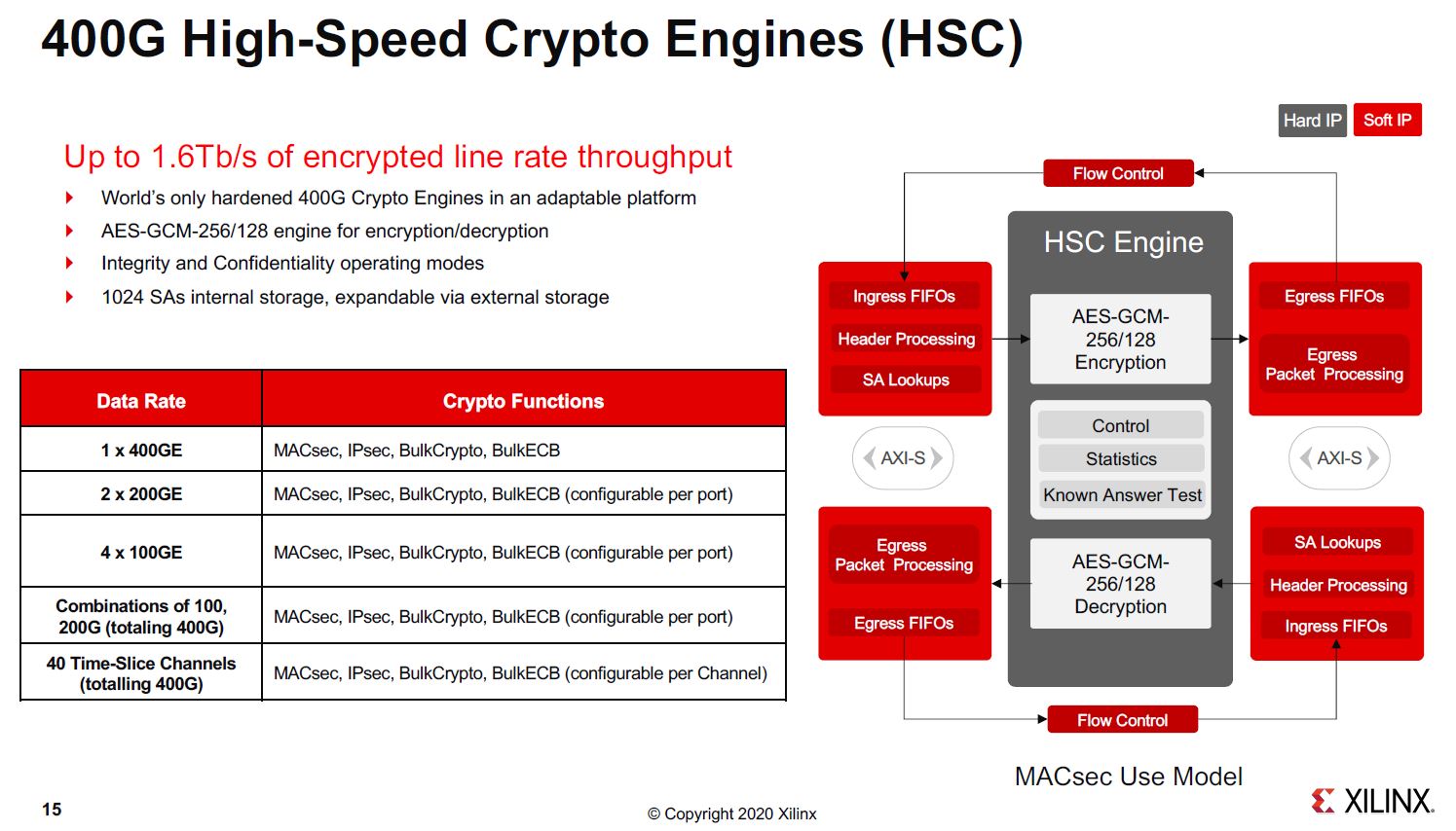
Since a lot of FPGAs are part of fabrics where crypto acceleration is important, Versal Premium has big hardened crypto accelerators that can handle the needs of 400GbE ports. For many applications that require high-speed crypto, adding a FPGA can be a flexible and easy way to add high-speed crypto where additional functionality can be added in the programmable logic even after deployment.
Getting data on and off the chip requires high-speed SerDes. Xilinx has a few solutions here including two different SerDes flavors.
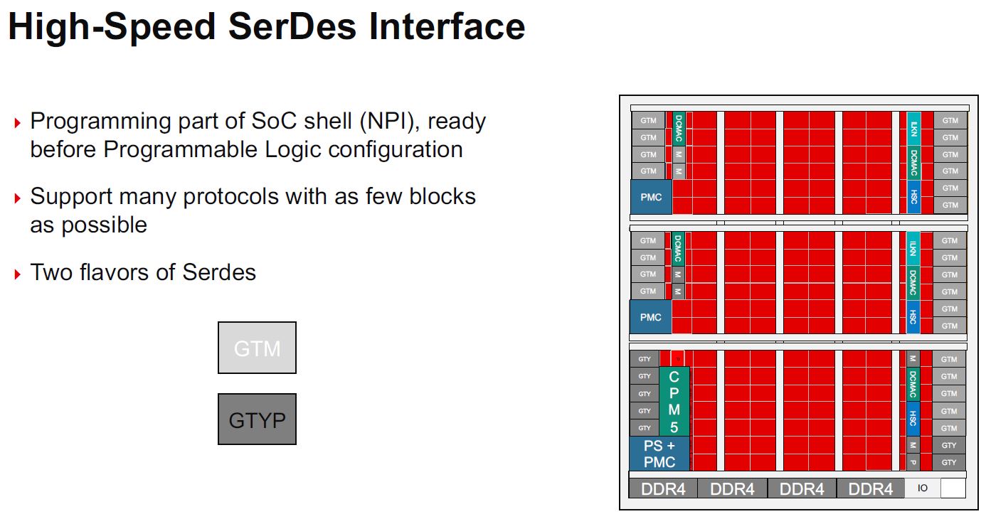
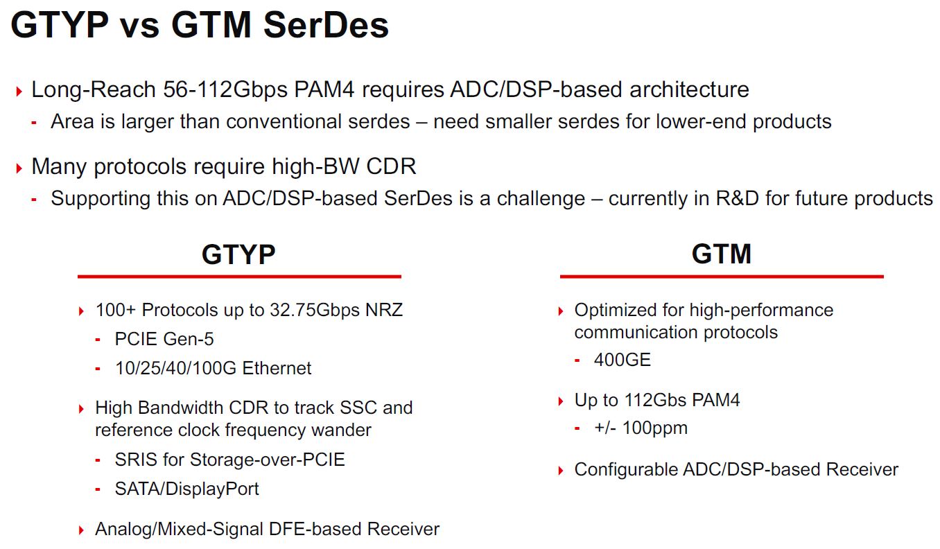
Xilinx has two different types of SerDes. There is a higher-end version as well as a more space-optimized solution. GTM is used for applications such as long reach PAM4.
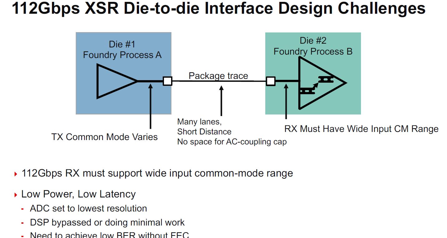
The 112Gbps XSR die-to-die interface is built to provide low power and low latency interfaces.
Here is the summary of Protocol Engines and SerDes. We will let our readers read this one.
We wanted to discuss a bit more in terms of connectivity.
Versal Premium PCIe Gen5, CXL, and CCIX
Xilinx Versal Premium has PCIe Gen5 and CCIX built-in. Xilinx was a major promoter of CCIX so we can see that integrated tightly in the FPGA.
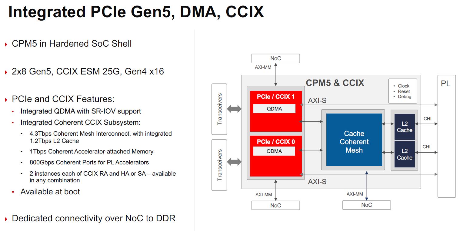
A second block is PL-based PCIe Gen5 and CXL. This is both hardened plus requiring programmable logic. As we get to the end of 2021, we are going to see a lot more on CXL. It seems like Versal was designed for CCIX, but then the industry moved to CXL between design and deployment. One of the cool features of a FPGA is that Xilinx can support CXL by moving some functions into the programmable logic.
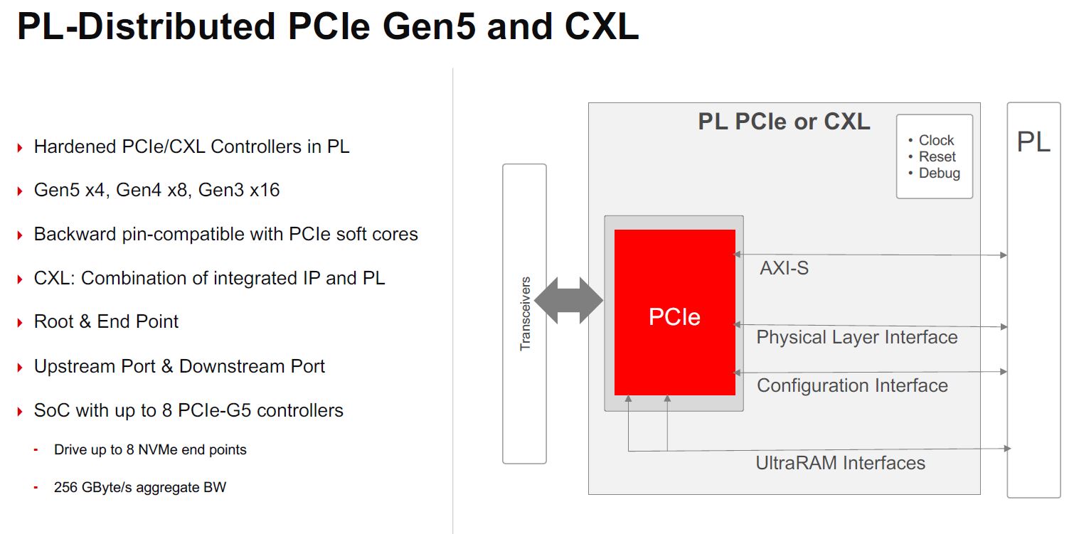
These are big chips, but we wanted to show off some of how the chips is built.
Building Versal Premium
A Versal Premium chip can hit up to 92B transistors by integrating multiple chips via the company’s Stacked Silicon Interposer Technology or SSIT. This utilizes TSMC’s CoWoS technology. If you want to see an early CoWoS implementation, a great example of the chips you can see in our piece How to Install NVIDIA Tesla SXM2 GPUs in DeepLearning12.
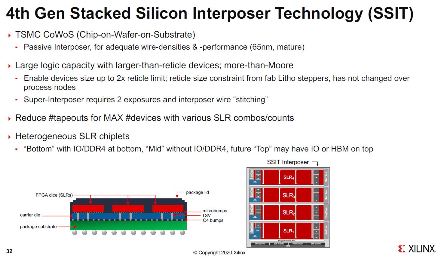
This approach allows Xilinx to create larger chips without having to necessarily create larger monolithic dies.
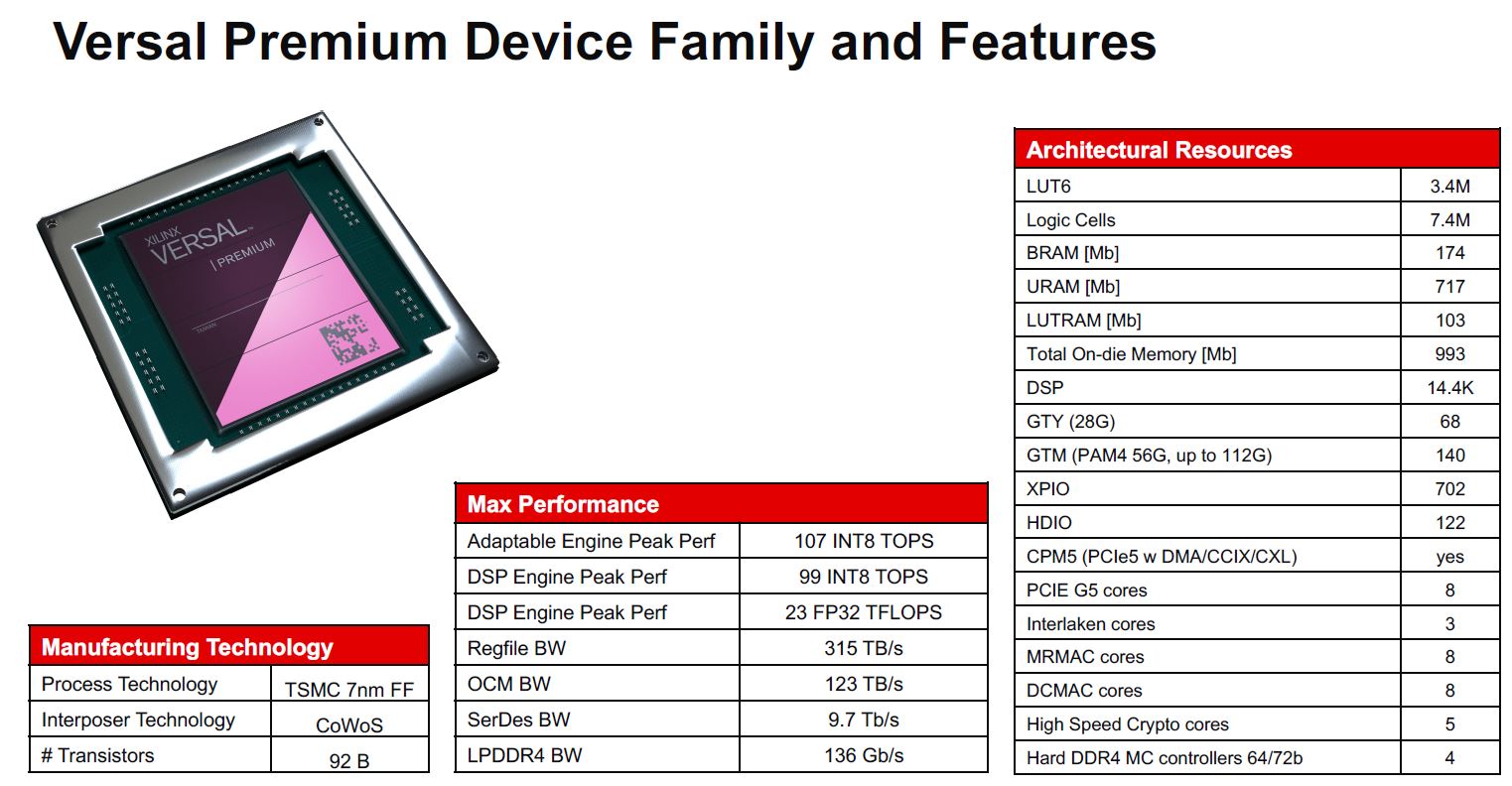
The Versal design scales up and down with connectivity and features. At the top end, there are certainly some big solutions that can be built.
Final Words
This is certainly an interesting solution. We have been working to show off some FPGA solutions in our lab as they go from requiring programming and integration knowledge to something more akin to a plug-in accelerator.
The big question is when these will start to ship in large quantities. Generally, Xilinx announces products well before availability. Still, the future of FPGAs is extremely exciting.

