Intel has been trumpeting the benefits of silicon photonics for well over a decade. It is to the point that engineers who started their careers at Intel somewhere in their 20’s hearing about silicon photonics for interconnects are now in their 40’s. Intel has long held the vision of disaggregated compute, storage, and memory sleds for the data center, connected via silicon photonics optics. During Intel Interconnect Day 2019, the company showed why its photonics have moved from a lab project to shipping in volume.
Intel Silicon Photonics Update at Interconnect Day 2019
Intel’s new VP of the group, Hong Hou, first set up the discussion with market forces driving the industry to silicon photonics, and why the concept has become a big talking point in the networking industry.
Instead of talking about exotic disaggregation, the opportunity laid out was more straightforward. With 100GbE and future 400GbE networking, Intel’s silicon photonics transceiver business has a growing market, and that market is well-known.
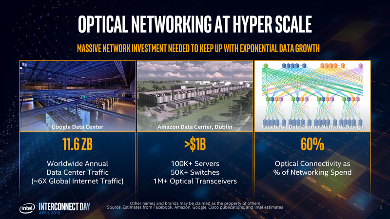
With faster networking standards, copper is challenged to deliver speeds over even in-rack distances. Anyone who has seen a 3m 40GbE v. 100GbE DAC will have noticed that the cable radius has gotten significantly thicker due to extra shielding with the newer generation. Not only is copper challenged, but multimode fiber will not reach across many racks as the industry moves to faster networking.
We were told that the various super 7 hyperscale companies have different strategies. Some tend to just set up whatever works and is the least expensive. Others, like Facebook, invest in single mode fiber to ensure the cabling infrastructure is ready for future upgrades over a data center’s lifetime.
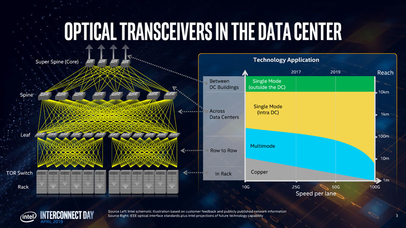
I had the opportunity to ask what the current ratio is at 100GbE. I was told that it is roughly 25% copper, 50% multimode, 25% single-mode fiber ratio being deployed. Intel now has about one-third of the 100GbE single-mode market. Those were off-the-cuff figures rather than exact numbers, but the point is that Intel’s silicon photonics is now shipping to the point where they have about one-third of the high-value single mode market.
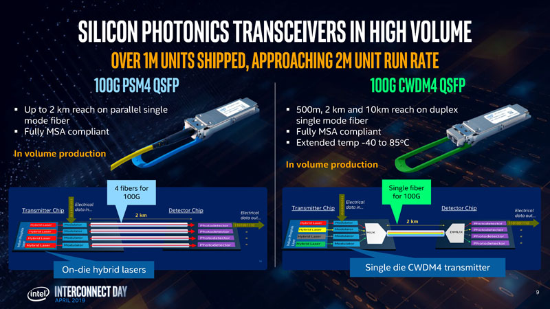
Intel claims that for the last six quarters, it has been the #1 provider of 100G CWDM4 QSFP pluggable optics.
Inside the Intel Silicon Photonics Pluggable Optics
Today’s Intel Silicon Photonics manifests themselves in pluggable optics. These are transceivers that sit in switches (and in theory NICs as well) to fire lasers over optical fiber cabling through a data center and between data centers.
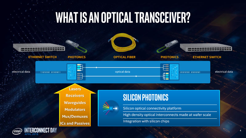
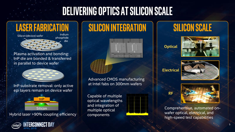
Silicon actually cannot be a light source, a requisite for building a laser. Instead, the company integrates an Indium Phosphide light source onto a 300mm silicon wafer. It then uses silicon to do modulation and other functions. Intel points out that its solution is the most integrated at this point and they are delivering the process at scale.
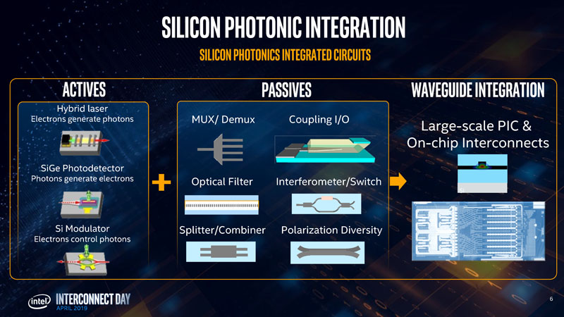
One of the key advantages to its silicon photonics is that with the integrated laser, photodetector, and modulator, it is also able to build into silicon many of the required passive functions into silicon making it a tightly coupled package.
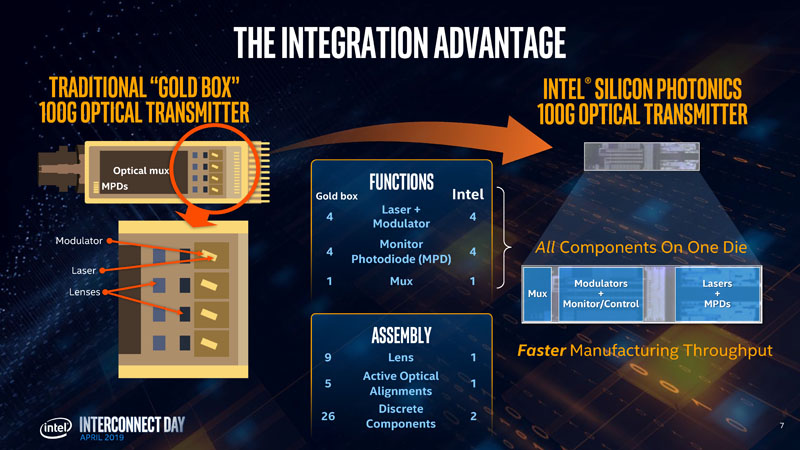
Current 100Gb optical transceivers need a labor-intensive “gold box” that needs to be carefully constructed with many different components (in this example 26) then hermetically sealed. In contrast, Intel gets the advantages of scaling through silicon process and the precision that brings. The silicon photonics package does not need to be hermetically sealed to operate in adverse conditions (e.g. humid deployments.)
Intel’s vision is that driving to silicon photonics means that it can build optics in volume. A hyperscale data center will consume around 1 million optics representing opportunities in the hundreds of millions to billions per data center deployment.
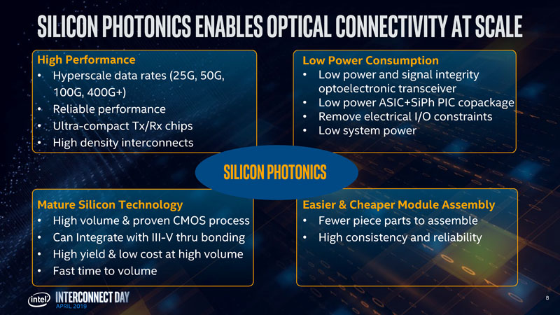
As we move to scale faster optics, Intel believes its solution is what will scale. Certainly, in the industry, there is now a lot of buzz around silicon photonics. There is so much power being used just to move data across PCB from the switch ASIC to the QSFP28 and QSFP-DD cages that packaging of optics will have to occur in a few years. At that point, the next-generation of silicon photonics like Intel is shipping today will become a necessity.
Moving to 400GbE and Why Silicon Photonics
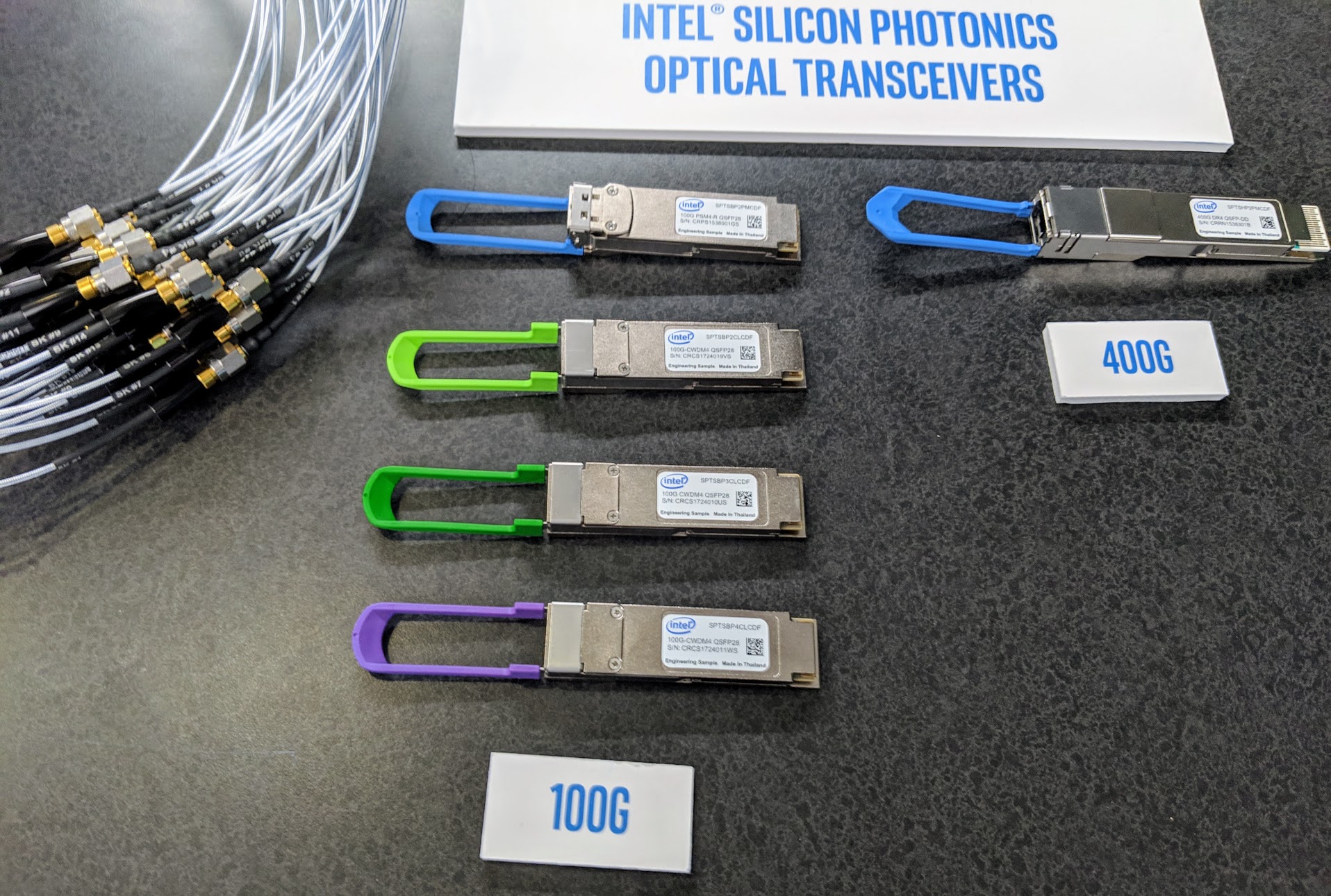
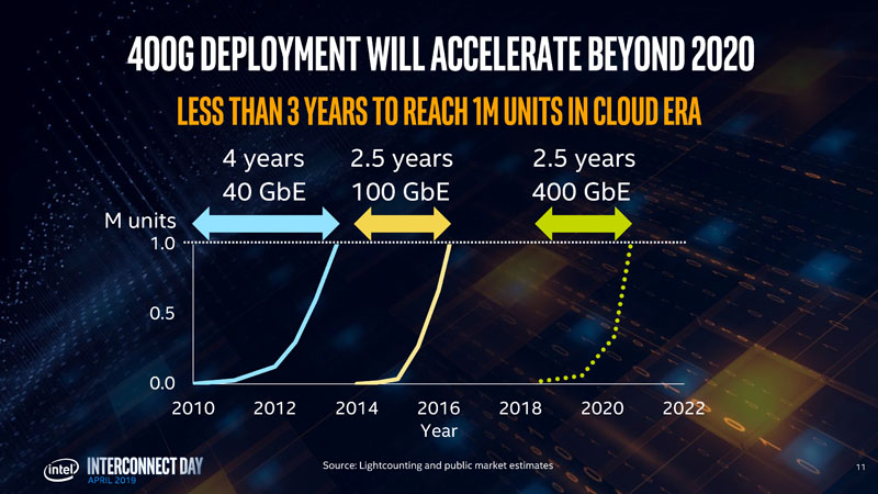
At OCP Summit 2018 and 2019, 400GbE is becoming a bigger push. We saw the Facebook Minipack Switch Partnering with Edgecore and Cumulus to bring 100GbE and 400GbE to the data center. 400GbE optics deployments are expected to reach 1M units shipped in the 2020 to 2021 timeframe. While the 40GbE ramp was relatively slow, the 100GbE ramp was much faster to hit 1M optics shipped and the 400GbE adoption curve will look more like 100GbE.
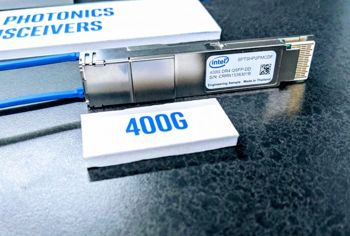
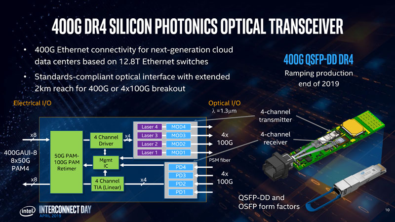
For this market, Intel has its 400G QSFP-DD DR4 transceiver. We are starting to see more QSFP-DD devices such as in our in-depth Dell EMC PowerEdge MX Review. Intel expects that this new transceiver will be in volume production by the end of this year.
The pluggable form factor is reaching some natural limitations. Although pluggable optics have been a foundational technology, they are hitting their natural limitations as speeds get faster. Starting with the 25.6Tb or 51.2Tb switch chips, we expect to start seeing co-packaged optics that we foreshadowed last year in pieces like our: Facebook Fabric Aggregator at OCP Summit 2018.
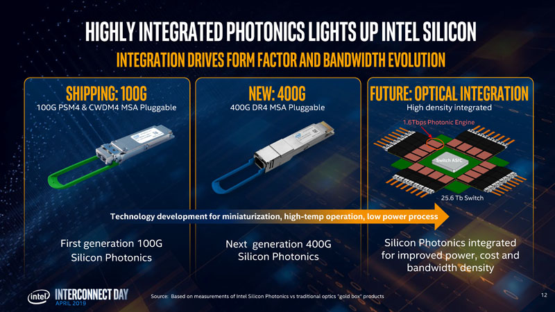
Intel thinks that in a world where it is building silicon chips with lasers and those chips need to be co-packaged with switch ASICs, that it has other technologies that can help the industry with packaging those solutions. Intel says it will be showing off this co-packaging in the first half of 2020 so this is coming in the next year or so.
Final Words
This is one of those technologies where the idea of moving chip-to-chip interconnects off of PCB and over optics is decades old. As we get to higher speeds, and power per bit moved becomes a bigger concern, we expect to see a greater focus on this area. For now, Intel is able to use the technology to fill a more traditional role for optics, and that is in pluggable form factors. A benefit here is that Intel is getting experience scaling technology and solving a real-world application with it today. We are still waiting for the future of Intel Xeon CPUs, FPGAs, memory, accelerators and other devices all connected via high-speed optics, and may be waiting for another decade. This gives Intel the practical application today to perfect the process and fund future development which is a natural progression for the technology.

