4th Gen Intel Xeon Scalable Sapphire Rapids: The Core
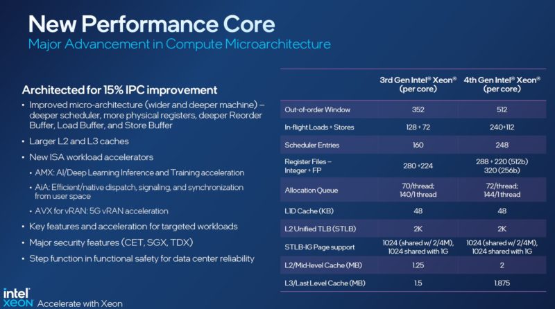
The core is Intel’s performance core codenamed “Golden Cove” which we have seen derivatives of before. There are a number of improvements throughout the core, but one of the other major differences are the caches. Intel is moving from 1.25MB L2 cache per core to 2MB, and then from 1.5MB of L3 to 1.875MB of L3 per core. Some parts may have more cache than cores. An example is the Intel Xeon Gold 6444Y which has 2.8125MB L3 cache per core. In the chart below, take the L3 cache to be a minimum figure on a per core basis and that 2.8125MB to be a maximum for public parts.
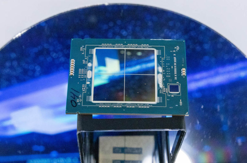
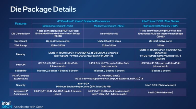
Previosuly we discussed the difference between the XCC and MCC packages. The MCC package is the traditional monolithic die. The XCC is something new. It integrates four compute tiles. It then uses EMIB to extend the on-tile mesh to adjacent tiles.
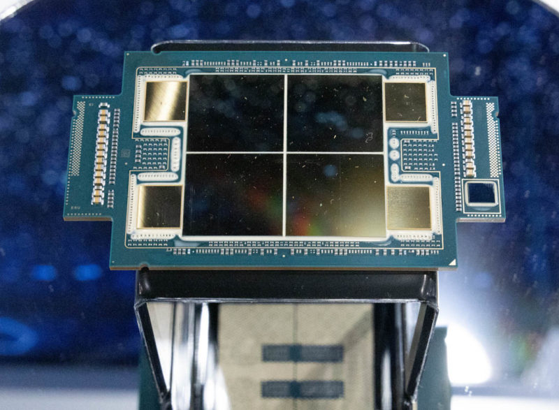
There is another variant of the XCC which is the HBM part. This integrates HBM2e memory on-package, and it is called the Xeon MAX. Each compute die gets its own HBM package.
Here are the diagrams for the three dies.
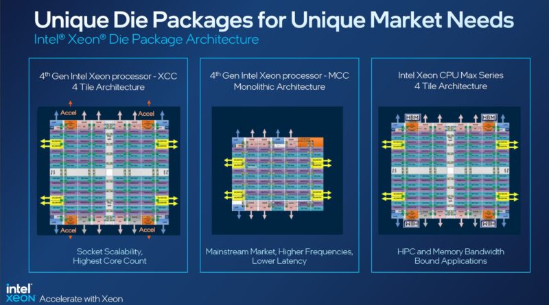
We have the larger versions of these images, but since we are not allowed to post them presently:
- Orange are the accelerator blocks
- Pink are PCIe Gen5 x16 /CXL 1.1 links. There is one that is a 1×8 Gen3 DMI instead
- Grey are inactive PCIe Gen5 x16 /CXL 1.1 links. On the XCC part, Intel has two not connected x16/CXL links
- The blue corers are x24 UPI links at 16GT/s
- Yellow are the DDR5 memory controllers, there are two controllers per XCC compute tile
- The teal/purple blocks are the cores and cache. On XCC, each tile is a 6×4 mesh. On MCC it is a 9×7 mesh
- One will note that the MCC die has 34 cores, but only up to 32 are active
Here are additional die package details:
Something that is notable is that 17 of the 52 SKUs are under 200W TDP, the minimum TDP for AMD EPYC 9004 Genoa.
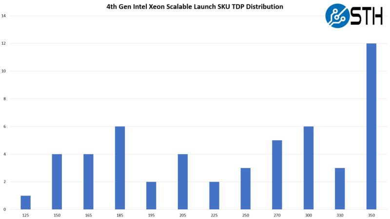
The advantage of Intel’s MCC design is that it can hit down to 125W, much lower than AMD is able to. We will quickly note that there is a C741 Emmitsburg PCH that adds some TDP to the system that AMD does not have since it is not using a legacy chipset approach.
Next, let us get to the platform and memory.


Wow … that’s a lot of caveats. Thanks for detailing the issues. Intel could really do with simplifying their SKU stack!
Not sure what to think about power consumption.
Phoronix has average power consumption reported by sensors that is ridiculously high, but here the peak power plug consumption is slightly less than Genoa.
Someone needs to test average plug power on comparable systems (e.g. comparable nvme back-end).
This is like BMW selling all cars with heated seats built into them and only enabling it if you pay extra.
Intel On Demand is a waste of engineering, of silicon, of everything, to please shareholders.
I’ve only made it to the second page but that SKU price list is straight up offensive. It feels like Intel is asking the customer to help offset the costs of their foundry’s missteps for the past four years.
The segmentation is equally out of control. Was hoping Gelsinger was going to reign it in after Ice Lake but I got my answer loud and clear.
New York Times: “Inside Intel’s Delays in Delivering a Crucial New Microprocessor
The company grappled with missteps for years while developing a microprocessor code-named Sapphire Rapids. It comes out on Tuesday.”
– NOT how you want to get free publicity for a new product!
I was so focused on Intel having fewer cores than AMD with only 60 I forgot that there’s still a big market for under 205W TDP CPUs. That’s a good callout STH
Intel did similar things when they lost track versus RISC/AMD back in the day. Itanium, Pentium IV (netburst), MMX and SSE were the answers they used to stay relevant.
P4’s overheated all the time (think they have this solved today with better cooling, but power is still a heavy draw).
MMX and SSE were good accelerations, complicating compilers and developers lives, but they existed on every Intel CPU, so you had a guaranteed baseline for all intel chips. Not like this mess of sku’s and lack of predictability. QAT has been around a while, and lots of software support, but the fact it’s not in every CPU holds it back.
The one accelerator that doesn’t need special software is HBM yet they limit that to too few SKUs and the cost is high on those.
This is not a win for Intel…this is a mess.
I’ve just finished reading this after 90min.
THAT is someone who’s got a STRONG understanding of the market. Bravo.
Where’s the video tho?
There is soomething wrong with the pricing for these products.
Especially with accelerators there is a price thing going on:
-QAT can’t compete with DPUs; as you mentioned those cost $300 more than a NIC
-AMX on $10k+ CPUs (with 56 or 60 cores) can’t compete with a $1500 GPU while consuming much more power than a CPU with less workload plus the GPU.
These sticker prices might not be end-prices. High core Genoa is also available now ~20% under MSRP from european retailers. I don’t really trust MSRP for this generation.
@Lasertoe – What we’re seeing here is the first step towards the death of the DPU. What is going to be ending it is when Intel integrates networking fabrics on package and thus you can dynamically allocate cores towards DPU tasks. This provides the flexibility, bandwidth and latency that dedicated external cards will quickly disappear.
Intel isn’t doing themselves a favor by having their on-die accelerators behind the On-Demand paywall.
Hello Patrick
I suspect you will earn lots of money if you could monetize your Intel SKU excel sheet :-)
How on Earth I can pick the best CPU for my workloads ?
Are there any tools that could identify which accelerations might be helpful for my workloads ?
Whole concept of the On Demand is kinda rotten.
I deploy the platform, I migrate the workloads, I realize that maybe some additional accel will be beneficial (how ?), I purchase the extra feature (and it won’t be cheaper if purchased from the get go), and then I need to trigger workload wide software refresh into acceleration enabled version ?
Hard to see that.
Sorry if the accelerators are meant to be decision factors there need to be widely adopted, they need to be a must, a no brainer. And they need to have guaranteed future.
I’m extremely confused how NONE of the “Max” SKUs are being offered with ANY of the onboard accelerators! (other than DSA, which seems like the least helpful accelerator by far.)
Is that a typo? The Max SKUs don’t even offer “on demand”?
@Kevin G:
I don’t think that will happen. I think Intel and AMD will both integrate DPU-like structures into their server CPUs.
Allocationg cores “towards DPU tasks” is already possible when you have an abundance of cores like Genoa (and even more with bergamo). The DPU advantage is that those (typically ARM) cores are more efficient, don’t need a lot of die area and don’t share many resources with the CPU (like caches and DRAM).
I can see a future where efficient coress with smaller die area like Zen4c or Atom (or even ARM/RISC-V) work along high-performance cores for DPU tasks but they need independent L3 caches and maybe DRAM.
Well, have to admit, I didn’t think there would be anything below the $1,500 mark. Granted, there’s not much, but a few crumbs. Now to see if you can actually get those SKUs.
Not buying the power levels until I see some actual test results. Frankly the lack of accelerators on so many of the high end SKUs definitely raises a few doubts as well. Why leave the thing you’ve been hyping up all this time from so many SKUs, and does this mean that there are, 4-5 different chip lines being manufactured? Thought one of the main angles was that they could just make a single line and bin those to make your variations and offer the unlocks to all the models?
Just waiting for all the “extras” to become a recurring subscription. You want the power efficiency mode turned on? That’s $9.99/hr/core.
“4th Gen Intel Xeon Scalable Sapphire Rapids Leaps Forward in Lead Times” Fixed the title for you ;)
Can anyone explain the difference between the Gold 5000 and Gold 6000 series? I can’t find any rhyme or reason to the distinction.
Adding to the confusion, the Gold 5415+ actually appears to be substantially worse than the Silver 4416+, and the Silver 4416+ costs $110 more. Why would a Silver processor cost more than a Gold processor and be better? There’s a pretty meaningless-looking distinction in base clocks, but given where the all-core turbo is at, I would bet that loading 8 cores on the 4416+ would yield clock speeds that aren’t far off from the all-core turbo clock speed of the 5415+… and then you still have another 12 cores you can choose to load up on the 4416+, with over 50% more cache!
The SKU matrix doesn’t seem very well considered. I also agree with Patrick’s comments on the confusing state of the accelerators; I think Intel should have enabled 1 of every accelerator on every single SKU, at a minimum. If they still wanted to do “On Demand”, that could allow users to unlock the additional accelerators of each type, but even having 1 would make a significant performance difference in workloads that can use them, and it would be an effective way to draw the customer into buying the licenses for additional accelerators once they are already using them.
Long. Superior article.
Intel should hire you to re-do Xeons products.
Will be interesting to see The hedt platform later how it Will perform campare to rapid lake ryzen and of course threadripper and also IF they have some new things outside of pci-e5 ddr5 or IF they cripple it as they did with x266
What an absolute mess. The naming has been awful since the whole “Scalable” marketing debacle but this is taking it to the next level. Was hoping they would sort it this generation. Sigh.
Patrick, any chance of testing a “fully populated” supermicro SYS-681E-TR? The mind boggles…
Accelerators have a chicken vs. egg adoption challenge. Intel hedged their bet with “on demand,” which makes adoption failure a self-fulfilling prophecy
I don’t know if anyone noticed, but in the chart on page 12 where Intel basically denounces the SPEC benchmarks they put “Gaming” twice in the “Customer workloads” set in relation to the release of a Xeon line.
A lot of games require servers for multiplayer gaming, don’t they? Then of course you have cloud gaming, which is much smaller, I’d imagine.
It does seem odd that they selected two customers with gaming workloads when there aren’t so many total.
“On Demand” is bullshit. It’s nothing more than artificial scarcity, a.k.a the Comcast model. I would be very angry if I paid for all of those transistors and over half of them were locked behind an additional paywall.
Thanks for the nice article. Unfortunately on general purpose computing it seems Intel is still trying to catch AMD and not successfully.
I’m using phoronix benchmarks geometric means (from set of benchmarks) comparison here with the specified CPU TDP, E.g. benchmark number / TDP = X. so this basically shows efficiency of processing in comparison with declared TDP. Higher number, better efficiency.
Intel 8280: 1.35
Intel 8380: 1.46 — looks like 14nm -> 10nm transition was moderately successful
Intel 8490H: 1.7 — again 10nm -> Intel 7 although it should be basically same, it looks like Intel did their homework and improved quite a lot.
AMD 9554: 2.3 — and this is from completely different league. TSMC simply rocks and AMD is not even using their most advanced process node.
Not sure if I get it right. It does seems like 8490H and 8468H had all accelerators enabled from the table you compiled
I don’t find these particularly compelling vs. AMDs offerings. The SKU stack is of course super complicated, and the accelerator story doesn’t sound very compelling – also raises the question if one can even use these with virtualization. And I don’t think most software supports the accelerators out of the box with the possible exception of QAT. The on-demand subscription model also bears the risk that Intel might not renew your subscription at some point.
Those SPECint numbers are ******* BRUTAL for Intel. I’m sure that’s really why they’re saying it’s not a good benchmark. If it’d been reversed, Intel will say it’s the best.
I’d agree on the speccpu #’s.
I read this. It took like 2hrs. I couldn’t decide if you’re an intel shill or being really critical of intel. I then watched the video, and had the same indecision.
I’d say that means you did well presenting both sides. There was so much garbage out there at least there’s one place taking up the Anandtech mantle.
Amazing review. It’s by far the most balanced on the Internet on these. I’ll add my time, it took me about 1.25 hours over 3 days to get through. That isn’t fast, but it’s like someone sat and thought about the Xeon line and the market and provided context.
Thx for this.
I think Intel is on the wrong path.
They should be making lower powered CPU’s.
Their lowest TDP CPU is 125W and its a measly 8 core, with a 1.9Ghz max boost frequency – I think something is wrong in Intel’s development department.
1.9Ghz boost frequency should not require 125W TDP.
What a hack was then when I tels Server market share was something like 97%
-what nonsense it still is ore than 90%
So how that affects anything
Data Center and AI (DCAI) $4.3 billion
Data Center $1.7 billion
That is Miikka maximum copium.
Patrick’s SKU tables show the 8452Y as MCC, but that’s clearly impossible since it has 36 cores. It should be XCC (which would also match Intel’s table).
I didn’t try to check all the others. :-)